Employing world-class nonferrous metal manufacturing technologies, we are a supplier of a wide variety of sputtering targets including for semiconductor applications, compound semiconductor materials, high-purity metals, and surface treatment. These and many other materials and services, provided on a global scale, find use cases in end products such as advanced devices, leading-edge IT equipment, medical instruments, and electric vehicles.
Nakamura Yuichiro
Director and Senior Executive Officer, General Manager, Thin Film Materials Division, Senior Executive Engineer, Technology Group
JX Nippon Mining & Metals Corporation
Against the backdrop of a growth in the overall size of the market driven by an accelerated digital transformation because of the COVID-19 pandemic, the increased demand from people telecommuting and demand from stay-at-home workers has meant an increase in the semiconductor sector-related market. With the aim of responding to future market trends for which further future growth is anticipated, we are implementing capital investments to improve our production capacity. We have decided to move forward with our plan to expand overall process facilities in production facilities for our product’s sputtering targets including copper, copper alloys, titanium, and tantalum used in forming ultra-fine interconnects for semiconductors that is part of our 2020-2022 medium-term management plan.
Nakamura Yuichiro
Director and Senior Executive Officer, General Manager, Thin Film Materials Division, Senior Executive Engineer, Technology Group
JX Nippon Mining & Metals Corporation
Fiscal 2021 will likely see ongoing uncertainty in the economic environment due to the widespread impact of COVID-19, the continuation of the United States’ hardline policy towards China, and the state of Korea-Japan relations. However, the normalization of economic activities through more widespread vaccination, accelerated efforts towards digital transformation by many companies, and the mainstream adoption of 5G, IoT, and ADAS (Advanced Driver Assistance Systems) mean that we expect to see an increase in demand for our products. Furthermore, we expect the need for advanced materials to grow further in the medium to long term. Accordingly, we will steadily implement previously decided capital investment and thus increase our production capacity in order to meet this demand, flexibly responding to customer needs that vary due to changes in the market, thereby gaining their trust.
Sputtering targets used for semiconductors are a mainstay product for the Thin Film Materials Business, mainly used in ultra-fine interconnects in leading-edge logic and memory chips, and demand for these continues to grow along with the move to a data-driven society. Factors such as telecommuting have resulted in increased demand for communications infrastructure and mobile terminals, and the semiconductor market is seeing accelerated growth. Looking forward, this underlying trend is expected to continue with the development of 5G and digital transformations.
We will enhance our production facilities for sputtering targets for copper, copper alloys, titanium, and tantalum used in ultra-fine interconnects for semiconductors, increasing our production capacity by 30% in fiscal 2020, and we are currently working on further expansion. We will continue our efforts to support expanded demand.
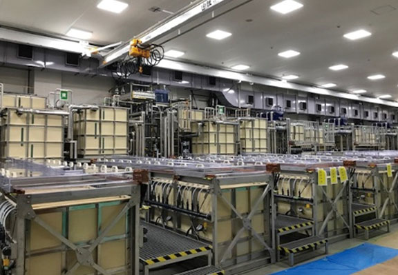
Production equipment used for semiconductor-grade sputtering targets such as electrolysis baths (Isohara Works)