Employing world-class nonferrous metal manufacturing technologies, we are a supplier of a wide variety of sputtering targets including for semiconductor applications, compound semiconductor materials, high-purity metals, and surface treatment. These and many other materials and services, provided on a global scale, find use cases in end products such as advanced devices, leading-edge IT equipment, medical instruments, and electric vehicles

JX Nippon Mining & Metals Corporation
Executive Officer, General Manager, Thin Film Materials Division, Senior Executive Staff, Technology Group
Suwabe Takeshi
Against the backdrop of growth in the overall size of the market driven by an accelerated digital transformation, the increased online-related demand resulted in growth in semiconductor-related markets. Amid this market expansion, fiscal 2021 saw continued strong demand for our mainstay products, such as sputtering targets for semiconductors, as customers increased production to cope with global tightness in semiconductor supply.
We had already increased our production capacity for sputtering targets for semiconductors in fiscal 2020, and have responded to growing demand by launching full-scale operation at these facilities. Furthermore, in order to meet current and future market needs, we have decided to further accelerate the expansion of our production system and reinforcement of our business foundation by launching construction of new plants around the world. We are also enhancing production capacity at our existing bases in a combined effort to significantly strengthen the production capacity of this product.
JX Nippon Mining & Metals Corporation
Executive Officer, General Manager, Thin Film Materials Division, Senior Executive Staff, Technology Group
Suwabe Takeshi
While there is continued expansion of digital transformation, the economic environment is becoming increasingly uncertain due to factors such as the global advance of inflation and Russia's invasion of Ukraine. However, needs for advanced materials from this division are expected to expand further in the medium- to long-term, especially in semiconductor-related markets, due to market growth expected in various areas, including the full-scale deployment of 5th generation (5G) mobile communication systems, the increasing use of electrical equipment in automobiles, and the expansion of electronic device use in relation to decarbonization.
To meet these growing demands, we will steadily implement capital investments, including the construction of new plants, to increase our production capacity and thereby justifying the trust of our customers. In addition to contributing to the achievement of the SDGs through our products, we also intend to meet society's expectations by keeping our attention on new development trends in response to various market changes and solving problems through internal and external collaboration.
Sputtering targets used for semiconductors are a mainstay product for the Thin Film Materials Business, mainly used in ultra-fine interconnects in leading-edge logic and memory chips, and demand for these continues to grow along with the move to a data-driven society. Factors such as telecommuting have resulted in increased demand for communications infrastructure and mobile terminals, and the semiconductor market is seeing accelerated growth. Looking forward, this underlying trend is expected to continue with the development of 5G and digital transformations.
After enhancing capacity by approximately 80% versus fiscal 2020 levels, we will continue our efforts to meet growing demand by enhancing our production facilities for sputtering targets for copper, copper alloys, titanium, and tantalum used in ultra-fine interconnects for semiconductors.
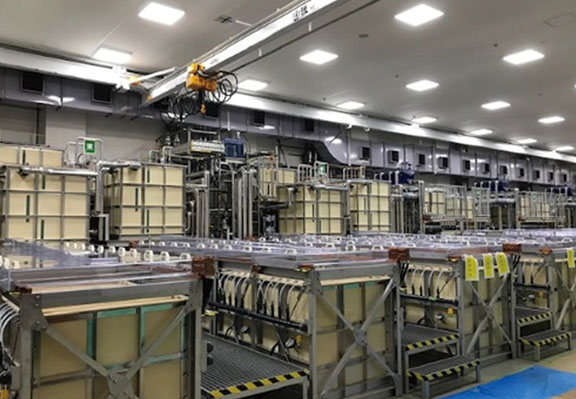
Production equipment used for semiconductor-grade sputtering targets such as electrolysis baths (Isohara Works)