Introduced here are the core technologies that comprise the source of our competitive strength,
accumulated over more than a century since our founding.
As we go forward, we will further promote collaborations with outside partners as well as evolving these
core technologies to provide new value to society.
- Refining
- Melting
Purification is demanded for metal materials used in the latest electronic parts, such as semiconductor devices where scaling continues to advance, reducing line width to the nanometer level. Equipped with our own proprietary refining processes for various metal materials, we are using them to provide materials with the world's highest levels of purity. These include pure metals that bring out the properties inherent in individual metals, and sputtering targets, for which such pure metals are raw materials.
Example of Technology
Molten Salt Electrolysis Method
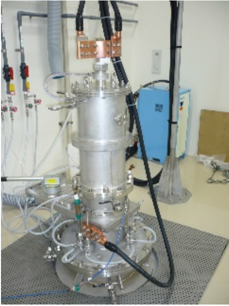
For metal elements that are not readily electrolyzed in a water solution, a process called molten salt electrolysis can be used for purification.
Typical Product
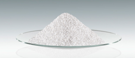
9N Cu
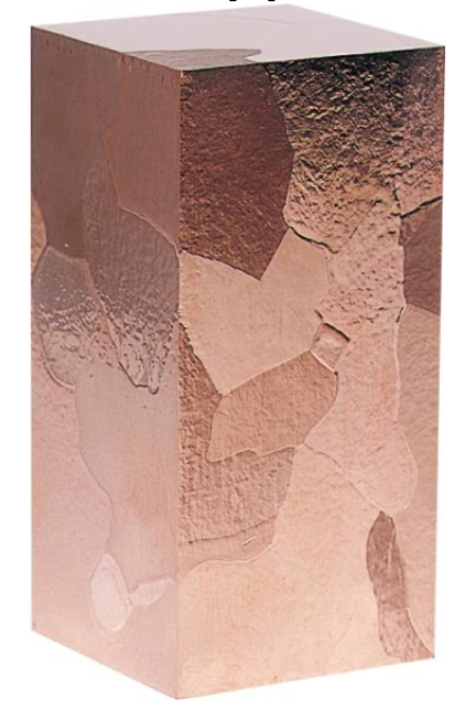
The world's highest purity
9N (99.9999999%) is achieved. Purification technology brings out the properties inherent in the metal.
Melting processes are essential to high-purity refining of metals. Different metals, however, have their own melting points and require their own specific melting technologies. What's more, contamination originating in the melting atmosphere or furnace must be prevented. We use many kinds of metal raw materials for a diverse range of purposes. We therefore have melting technologies for each of these purposes, which we use in a wide range of processes, from purification of the high-purity raw materials used in our own products to manufacture of the high-purity metals we supply to the market.
Example of Technology
Melting Equipment
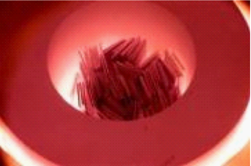
We have various melting furnaces in which we apply suitable melting methods for each element. Among them are vacuum induction melting furnaces, electron beam melting furnaces, and plasma arc melting furnaces.
Typical Product
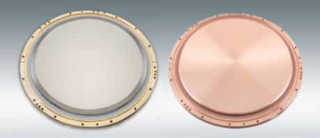
Sputtering Target (Ta)
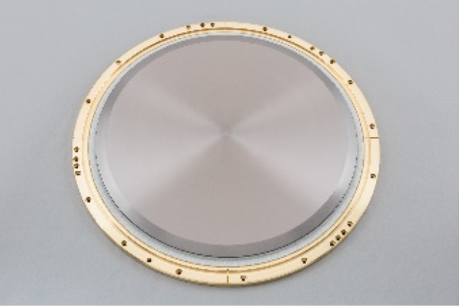
The melting processes enable us to provide sputtering target with purity of 6N (99.9999%), well above the industry standard.
- Metals, Alloys, and Composites Design
- Ceramics Design
- Single Crystal Growth
The properties and quality of advanced metallic materials are affected not only by their composition and purity, but also by the crystal grain size and the crystal orientation. This is not simply a matter of small crystal grain size or uniform orientation being best. The ideal crystal structure differs depending on the application. Based on the manufacturing knowhow and simulation technology we have developed over the years, we study alloy composition and crystal structure, and combine our proprietary rolling and annealing process technologies to achieve the required properties.
Example of Technology
Microstructure Control of Alloys
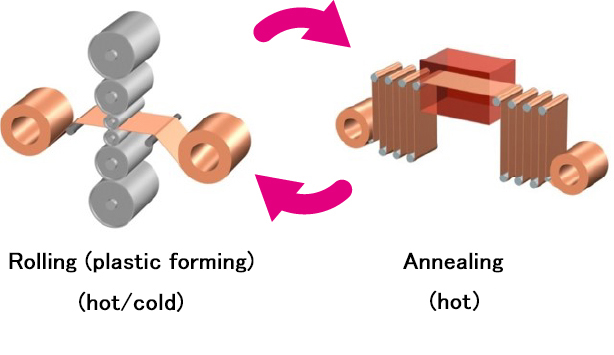
Alloys are produced by repeated processes of rolling and annealing. By optimizing the rolling and annealing conditions, the size and the orientation of the crystal grains are controlled.
Typical Product Application
Treated Rolled Copper Foil for FPC (HA, HA-V2)
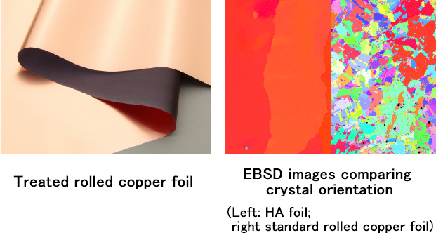
Bendable flexible printed circuits require flex capability in the copper foil used for their interconnects. A large grain size and highly cubic orientation result in copper foil that can be bent without a crack.
In the manufacture of ceramic materials such as ITO (Indium-Tin-Oxide) sputtering target for transparent conductive film, we are able to control the grain size by performing all the processes in house, starting from raw materials. Then we provide high-density, high-quality ceramic materials by utilizing the best processes for each material, such as high-pressure sintering.
Example of Technology
Hot Press
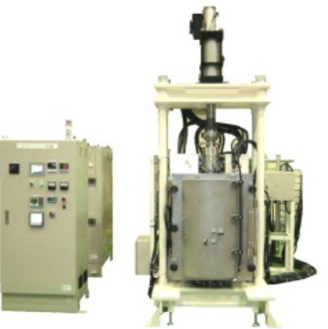
This equipment can perform high-temperature, high-pressure sintering in a vacuum or inert gas atmosphere. We have a large variety of hot press equipment, for uses from testing to manufacturing, and can select equipment of the desired size.
We manufacture single crystals for compound semiconductors by means of the melt growth process. From among the various methods for growing single crystals, we select a method optimal for each product. In the crystal growth stage, we optimize the growth conditions and temperature profile to manufacture compound semiconductor ingots with large diameter, few crystal defects, and uniformly distributed dopant concentration, providing high-quality compound semiconductor substrates. Of these, our InP products, widely recognized for their quality, have captured a large market share in applications such as optical communications supporting the IoT era.
Example of Technology
LEC (Liquid Encapsulated Czochralski) Method
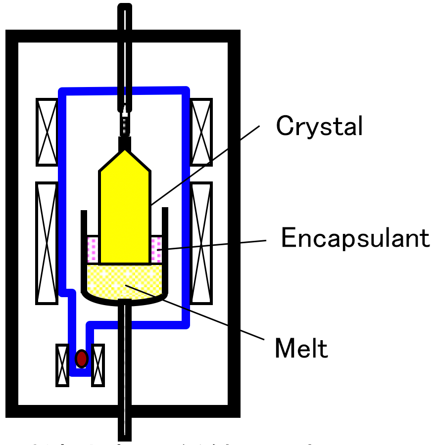
In this single crystal growing method, a seed crystal is dipped from above into the melt and is slowly withdrawn while rotating. The surrounding melt surface is encapsulated in a liquid to prevent evaporation from altering the composition.
Typical Product Application
CdZnTe Single-Crystal Substrate
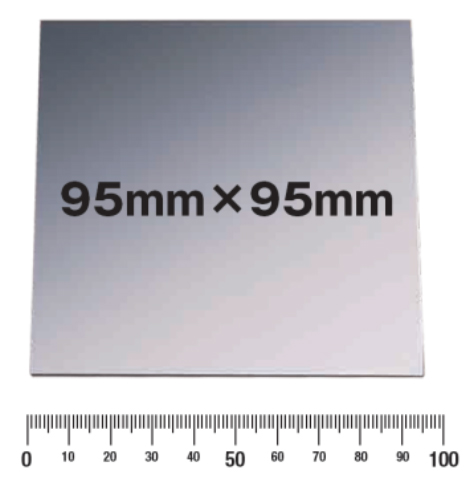
A compound semiconductor substrate being studied for use in infrared or radiation detectors. Along with the world's largest size, it boasts high quality including uniform in-plane concentration distribution of the Zn additive.
- Powder Manufacturing
- Powder Handling
We manufacture a variety of powders, from those used as raw materials in our own products to powders supplied to the market. They include metallic alloys, oxides, and other materials. Their applications are also broad, ranging from metal additive manufacturing to raw material powders for sputtering targets made using powder metallurgy technology. We have powder manufacturing technology, including wet and dry methods, appropriate for each of the materials and products. We can also meet customer needs for powders with advanced functions: our technology extends to control of grain diameter and to creation of special functions through surface treatment.
Example of Technology
We have various equipment required for powder manufacturing, such as gas atomizers and jet mills, and it is possible to select the process according to the desired quality.
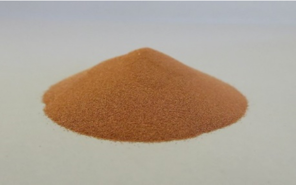
Typical Product Application
Sputtering Target (Tungsten)
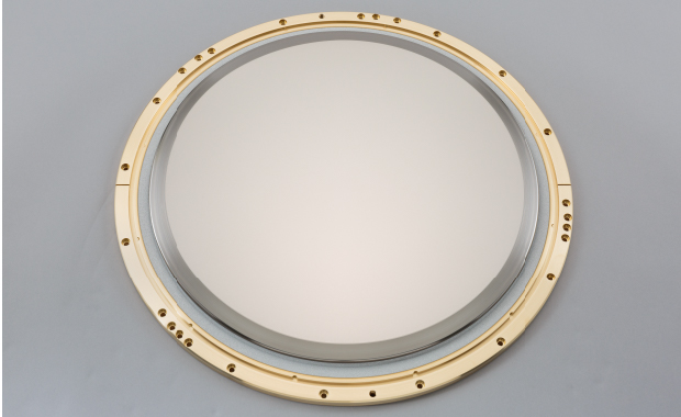
By means of advanced powder synthesis and milling processes, we are able to provide sputtering target with high purity (5N) and fine microstructure.
We handle metals, oxides, and other powders of various diameters and shapes. The particle size distribution of these powders should be controlled broadly or sharply depending on the application. Moreover, handling powders with grain sizes from the nanometer- to sub-micron meter-level, requires dealing with issues such as particle aggregation (flocculation). For these issues, we have various powder handling technologies such as improving powder dispersibility and granulation.
Example of Technology
Milling, Granulation, Classification
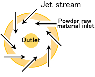
Jet mills, which improve dispersibility by milling various metal powders, are used in powder manufacturing processes.
- Rolling
- Accurate Bulk Machining
Our rolling technologies are used for manufacturing a wide range of products. These extend from rolled copper foil, made using the world's only integrated production system starting from the copper resource development stage, to sputtering targets made from the ingot stage. Since the final target thickness is achieved by rolling in multiple passes, variations in the in-plane thickness during one rolling pass will appear as large variations in the final product. By improving the entire process in addition to the rolling mills, we have succeeded in establishing mass production technology for rolled copper foil of 5 μm, the world's thinnest.
Example of Technology
Precision Rolling
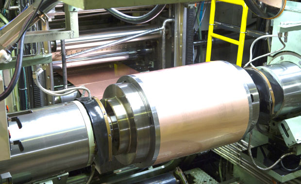
We use integrated process management to manufacture ultra-thin, flat rolled copper alloy foils, incorporating our original expertise and making use of custom-made rolling mills and annealing processes.
Typical Product Application
Titanium Copper Foil
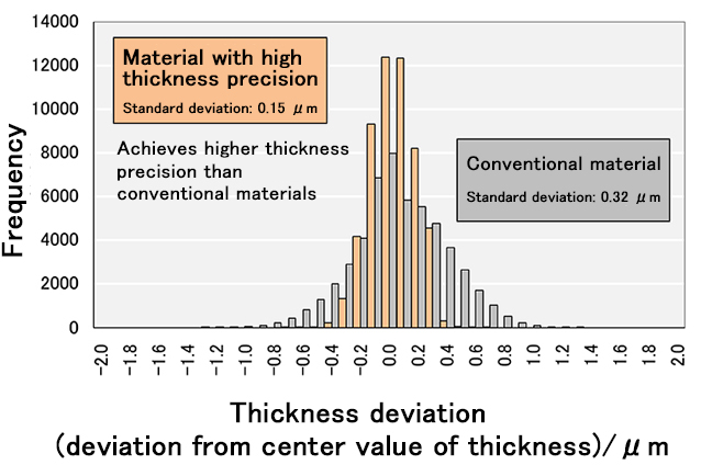
Titanium copper, one of the hardest copper alloys, is rolled to produce a foil with a thickness of 30 μm. The thickness deviation is only around ± 0.2 μm, well below the tolerance of 1% or less.
Compound semiconductors are made from monocrystalline ingots, processed and shipped as substrates providing the thickness and flatness required by customers. Methods of cutting substrates from ingots include using a multi-wire saw or an inner-diameter saw. We use a multi-wire saw for high production efficiency. Since flatness in particular affects yield in the customer's final processes, it is important to meet the required specifications. Along with this cutting technology, we provide extremely flat compound semiconductor substrates by means of a downstream polishing process.
Example of Technology
Multi-wire Saw
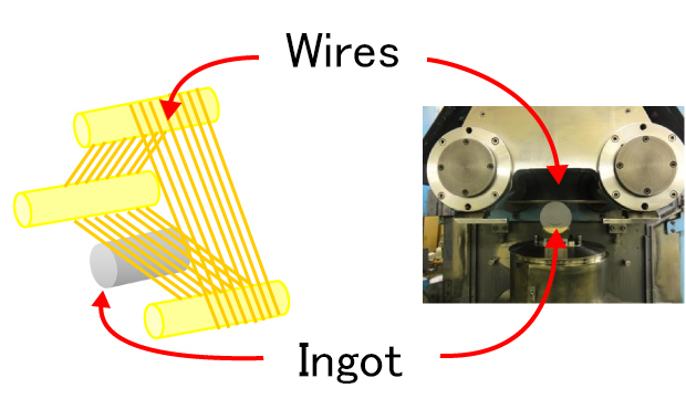
Abrasive grains are supplied as the wires are driven at high speed, cutting the ingot into wafer shape with a minimum machining allowance.
Typical Product Application
InP Substrate
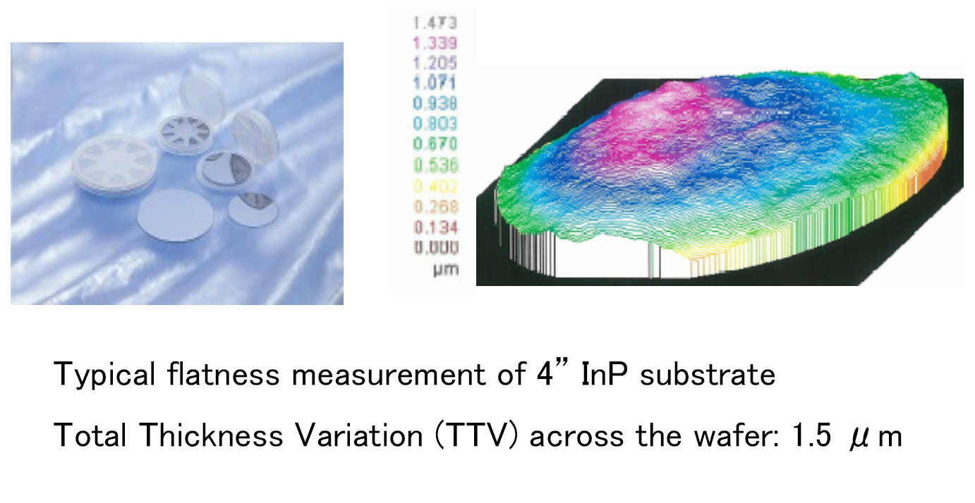
We provide extremely flat substrates matched to the exposure precision demanded in the photolithography process.
- Polishing, Etching, and Cleaning
- Surface Deposition and Plating
- Surface Treatment
- Adhesion, Bonding, and Compositing
For the sputtering targets and other materials we provide, manufacturing efficiency in customer processes is affected not only by the material composition and purity but by the surface properties. In the final process before shipping, therefore, we process the materials to provide the required properties, from surface roughening by etching to mirror finishing.
Example of Technology
Chemical Mechanical Polishing (CMP)
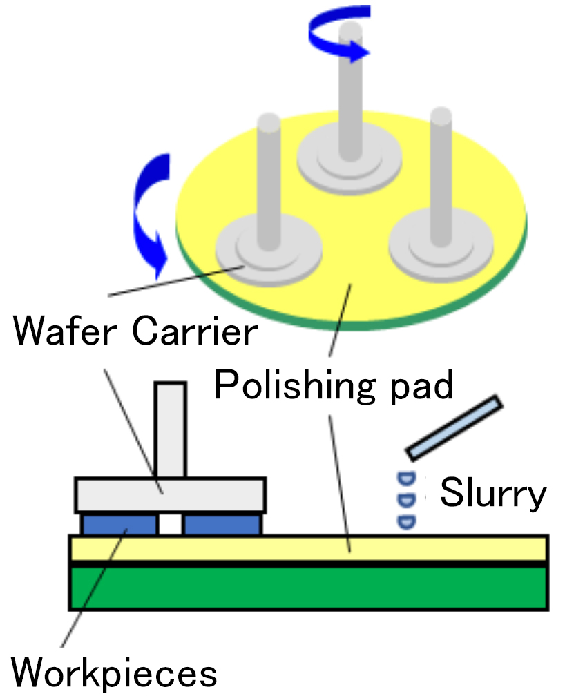
The workpieces are polished by the chemical action of the slurry and the mechanical action of the polishing pads and abrasive component, resulting in few defects and high precision.
Typical Product Application
SR (Sputter Ready™)
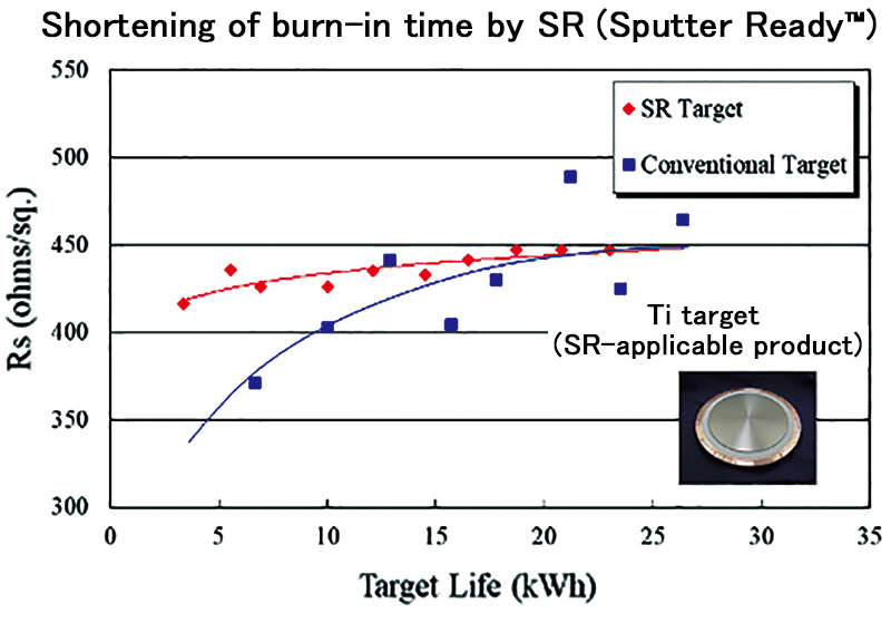
By making the product surface as flat as possible, arcing and other quality issues in sputtering are reduced.
We have our own technologies for both electrolytic and electroless plating, and the capability for high-precision plating at the micron level with either method. These technologies are used widely, from roughening treatment for improving the peel strength of copper foil to the substrate, to fine electrolytic plating on metal parts and our electroless plating services for semiconductor wafers.
Example of Technology
Electroless Plating (UBM)
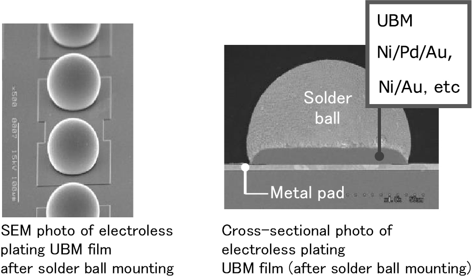
UBM (Under Bump Metallurgy) is plating film applied to semiconductor wafer bonding pad and solder joint areas. At our cleanrooms in Taiwan and Japan, we use an electroless plating process we developed in house to provide processing services in line with customer needs.
Typical Product Application
Copper Foil: BHM Treatment

Our surface treatment technology has achieved low transmission loss at high frequency bands while maintaining high peel strength, as well as improving surface flatness. Furthermore, by improving the surface treatment material, we can also enhance etching properties, enabling finer circuit patterning.
Various kinds of surface treatments enable us to maintain the original functions of a material while providing the unique functions required, ranging from prevention of oxidation for copper foil to control of sintering behavior for metal powder.
Example of Technology
Sealing Treatment for Gold Plated Film
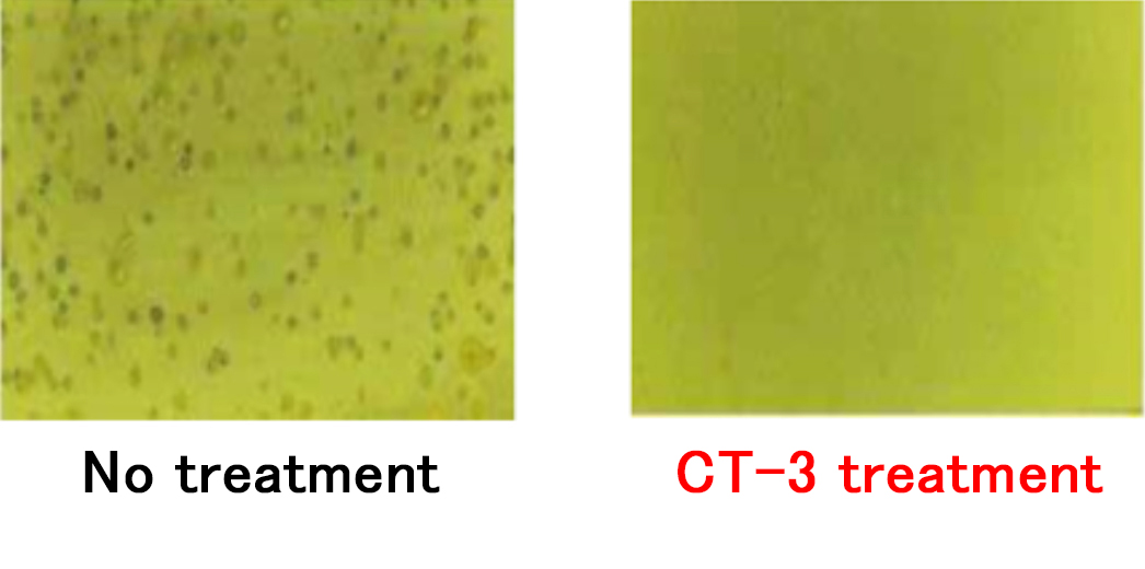
Pit corrosion can be prevented even in corrosive gas by forming an organic treatment film with thickness of approximately 2 nm on the surface of gold plated film.
Typical Product Application
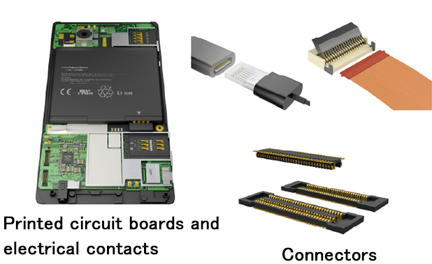
Good conductivity for wiring and connector pins can be maintained by anticorrosion treatment.
Sputtering targets are attached to a base—normally a backing plate or backing tube—for installing in the sputtering equipment. If the bonding of the sputtering target to the backing plate is not sound, the temperature of the target surface during sputtering will not be uniform, leading to various problems. Uniform bonding strength is achieved by technology suited to each kind of material, such as use of solder or diffusion bonding between different materials. In addition, by applying technology for bonding different materials, we are developing new materials such as composites of copper foil and resin.
Example of Technology
Solder Bonding and Diffusion Bonding
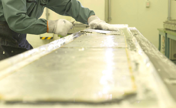
The solder bonding technique is suitable for any kind of material, even brittle material. Although diffusion bonding cannot be suitable for all materials, it offers high bonding strength and reliability.
Typical Product
Sputtering Targets
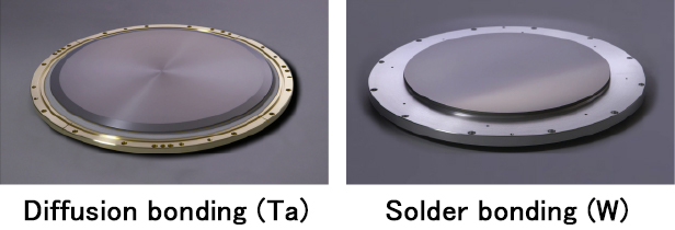
Our sputtering targets for semiconductors are bonded to backing plates. Our lineup includes solder bonded targets, diffusion bonded targets, and also monolithic targets, depending on the material.
- Inorganic and organic Analysis
- Surface Analysis and Structural Analysis
- In-house Evaluation
- Computer-Aided Engineering and Materials Informatics
Analysis technologies are fundamental technologies essential to our business activities in quality assurance, raw material evaluation, process control, research and development, and environmental evaluation. For this reason, we are working not only on introducing the latest analytical equipment but also on developing analytical technology. For development and quality assurance of high-purity metals, for example, we are strengthening analysis technology relating to glow discharge mass spectrometer (GDMS) and inductively coupled plasma mass spectrometry (ICP-MS) equipment. Along with the latest analysis technologies such as these, we also value classical technologies such as fire assay of gold and silver, for their high precision and accuracy.
Examples of Inorganic and organic Analysis Technology
GDMS and Typical Lower Detection Limits
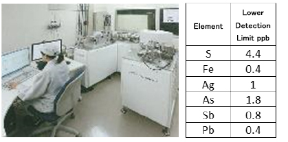
We have the largest collection of GDMS equipment in Japan. This equipment supports our development of high-purity materials by measuring the amounts of trace impurities.
ICP-MS/MS
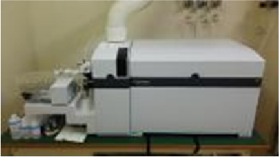
We have introduced the latest ICP-MS system, namely, ICP-MS/MS, which is less subject to interference by coexistent elements than earlier systems.
Fire Assay
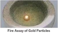
Fire assay is an analysis method based on gravimetry, and even though it takes a great deal of time and effort, it is characterized by high precision and accuracy.
We observe and analyze materials using the latest equipment, including devices for scanning electron microscopy (SEM), scanning transmission electron microscopy (STEM), mineral liberation analysis (MLA), X-ray photoelectron spectroscopy (XPS), and auger electron spectroscopy (AES). With STEM, we utilize the ultra-high resolution of 1 nm to investigate the structure of compound semiconductors and sputtered films, and clarify the function expression mechanisms of advanced functional copper alloys. We are also working to improve our capability for identifying compounds (minerals). With MLA, we are able to learn about the average composition of the ores by analyzing tens of thousands of tiny particles embedded in resin, improving the efficiency of resource development and of smelting and refining processes.
Examples of Surface Analysis and Structural Analysis Technology
Using STEM to Evaluate Osmium Vapor Deposited Film
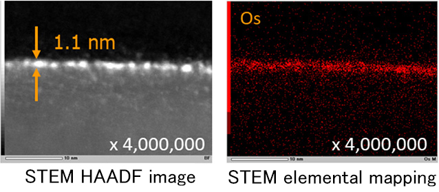
This is an example of analyzing osmium vapor deposited film formed on a silicon substrate at the 1 nm level. With STEM, even ultra-thin films of 1 nanometer can be analyzed.
Using MLA to Analyze the Average Composition of Ore A
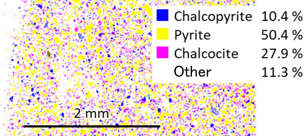
Using MLA to perform wide-ranging analysis of ores, we have succeeded in analyzing the distribution and average composition of each type of mineral. Normally, tens of thousands of particles are analyzed all at one time.
Our products are used as materials in customer products. By evaluating our products under the conditions in which they are used by the customer, we ensure that the expected functions and properties are present in the final form.
Examples of Technology for Evaluation in Actual Use Environment
Sputtering Deposition Evaluation
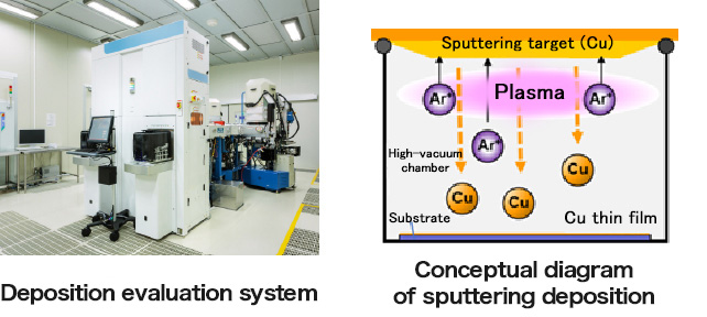
In sputtering, atoms ejected (“sputtered”) from the target accumulate on the substrate, forming a thin film. As we can conduct sputtering tests in house for our products, we confirm sputtering performance and thin film properties in order to improve target quality and performance.
FPC Bending Test
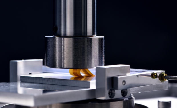
Since flexible printed circuits (FPC) are bent into small spaces, it is vital not to generate any cracks in the circuits. We perform bending tests under actual FPC use conditions to confirm that our copper foils can fulfill the bending requirement.
Besides having our own simulation and data analysis technologies, we collaborate with outside companies and research institutions to enhance those technologies. Use of these computer science technologies is helping us to design new alloy compositions and improve quality.
Example of Computer-Aided Engineering
Using Thermodynamic Analysis to Seek New Alloy Compositions
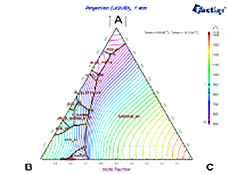
We develop and manufacture various leading-edge materials matched to customer needs. Using thermodynamic analysis tools during the alloy design process, we can conduct comprehensive searches for alloy compositions of three elements, and of four or more elements, thereby speeding up development and ensuring product implementation.
Example of Materials Informatics
Using SVM for Manufacturing Process Optimization
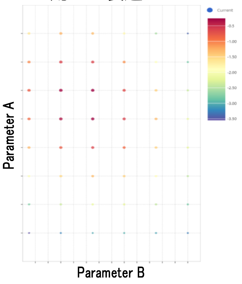
As production sites are evolving into smart factories, various analysis methods are being applied to the massive amount of manufacturing data obtained, such as decision trees, Bayesian optimization, and deep learning, yielding benefits in quality improvement. The figure shows an example of using a Support Vector Machine (SVM) approach to optimization of manufacturing process conditions.
- Mineral Resources Exploration and Development
- Smelting and Refining
- Recycling
- Safety and Environmental Cleaning
We have invested in some of the world's leading copper mines, including Los Pelambres and Escondida mines, as well as the wholly Japan-funded Caserones Copper Mine. Boasting equity entitled copper mine production of approximately 200,000 tons annually (2018 output), they are helping to ensure a stable supply of copper resources for use in products essential to daily life, from wires and cables to electronic parts.
Technology Development in the Copper Mining Industry
The JX-Iodine Process
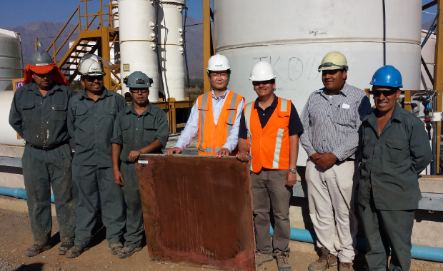
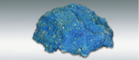
We developed an original process using iodine for recovering copper from low-grade sulfate copper ores. We conducted a pilot trial of this process in Chile, verifying its practical feasibility and effectiveness in improving copper leaching performance. We are now seeking to make use of the trial results to put the process to practical use in mines.
Copper Resource Development Site
Caserones Mine
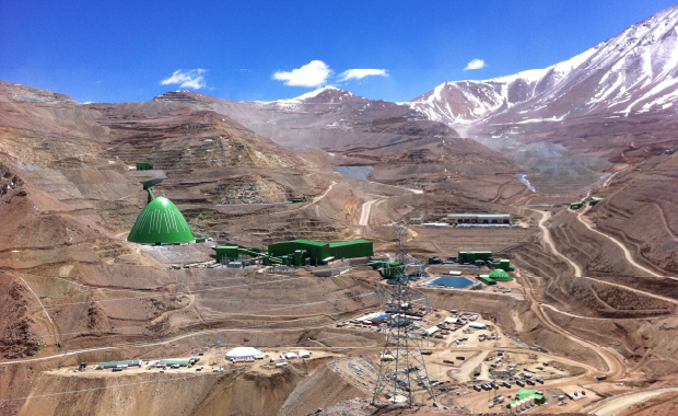
The Caserones Copper Mine in Chile is operated as an all-Japan-funded project led by the JX Advanced Metals Corporation Group. Production of refined copper by the SX-EW method (30,000 t/year) began at the mine in 2013, followed by copper concentrate production (150,000 t/year) in 2014. The mine is expected to have a production life of 28 years, lasting through the year 2040.
We have many unique smelting and refining processes, including use of a concentrate burner and a hydrometallurgical anode slime treatment process adopting solvent extraction. Besides using these processes for smelting of copper concentrate, we contribute to society by using them also for treatment of electronic scrap and other recycled materials, as well as for stable supply of refined copper (99.99% purity), precious metals, minor metals, and sulfuric acid. As one of the world's leading smelting and refining companies, we are also actively engaged in environmental protection, such as power generation through recovery of waste heat.
Examples of Copper Smelting and Refining (Pyro- and Hydrometallurgical Refining) Technologies
Concentrate Burner for Flash Smelting Furnace
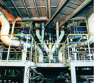
We developed our own concentrate burner with excellent reactivity, using the excess heat from an oxidation reaction of copper concentrate to melt recycled materials. We are also actively utilizing waste heat recovered from various processes for efficient power generation, contributing toward realization of a resource-recycling society.
Precious Metals Recovery Process
Hydrometallurgical Processing of Copper Anode Slime
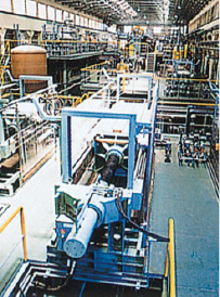
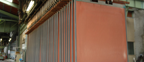
Electrorefining is used to produce 4N refined copper. We also developed the world's first high-efficiency hydrometallurgical anode slime treatment process (including solvent extraction), which is used to produce precious and minor metals from copper anode slime.
Saganoseki Smelter & Refinery
Overall View

This smelting and refining facility is located on the Saganoseki Peninsula (Oita Prefecture), known for its “Seki” brand mackerel, horse mackerel, and yellowtail. At the city of Hitachi in Ibaraki Prefecture, where our company got its start, we still have an operating site actively engaged in business. It is the setting of Jiro Nitta's novel, A Town and a Tall Chimney, and continues to uphold our corporate philosophy of realizing a sustainable society.
We provide recycling services, making use of smelting and refining technologies to efficiently recover copper, precious metals, minor metals, and other resources from recycled materials. We also provide environmental services including zero emissions processing of industrial waste to render it harmless without producing any secondary waste. We established the Hitachi Metal-recycling Complex (HMC) Department in the Hitachi Works, engaging in the recovery of a wide variety of valuable metals. At the same time, we have been taking steps to strengthen the network linking us to recyclers and hydrometallurgical refiners for collection and processing of recycled materials.
Example of Technology
Lithium-ion Battery Recycling
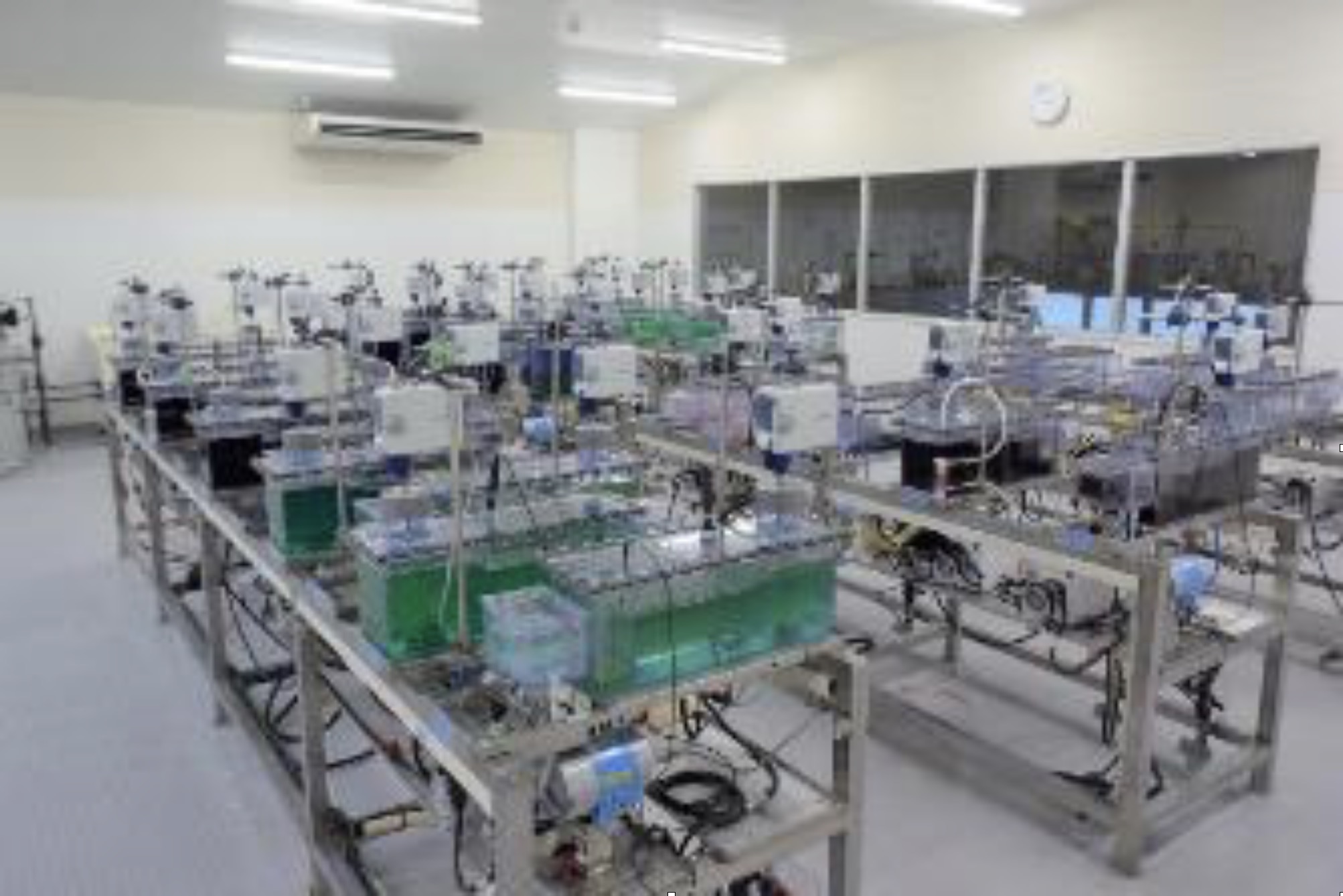
In the Hitachi Works, we have begun a recycling trial project to verify recycled materials that can be mass produced and their quality, using as raw materials the spent automotive lithium-ion batteries and process scrap provided by car and battery manufacturers. In addition to metal salt, samples of various properties and states including solutions and metals can be manufactured in line with customer needs.
Example of Recycling Site
JX Metals Circular Solutions
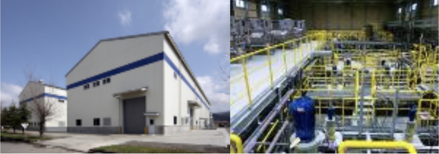
JX Metals Circular Solutions is conducting plant-scale verification tests of LiB recycling and has established technologies to recover metals from consumer LiBs. Since 2021, the company has conducted verification tests to recover high-purity metal salts that can be used directly as a raw material for positive electrode materials, with the aim of demonstrating closed-loop recycling of EV LiBs. At the same time, the company is also developing LiB pretreatment technologies suitable for our wet metal recovery processes.
We consider it our obligation as a member of society to give the highest priority in our business activities to environmental measures and safety, including that of our employees. This thinking began with the construction of the giant stack to deal with smoke pollution from the Hitachi Mine, the Company's birthplace, and has continued to be passed down for more than a century since that time.
Example of Safety and Environmental Cleaning Technology
Acid Mine Drainage (AMD) Treatment at Closed Mines
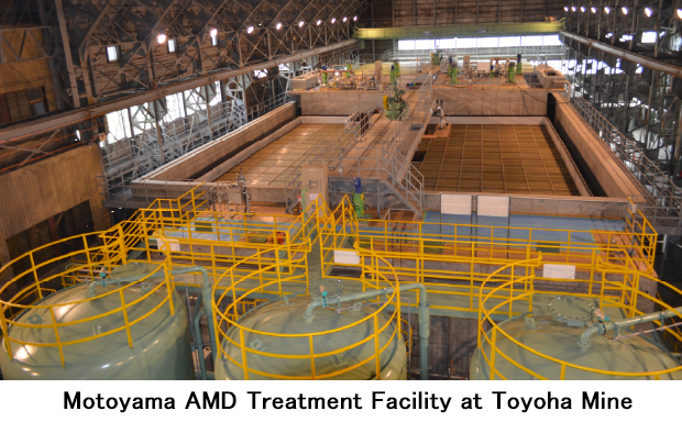
Mine drainage consists of pit water rising up from inside the mine and effluent discharged from tailings dams or other mine facilities. It occurs when rainwater and other water comes into contact with materials such as ores remaining after the mine is closed. As this drainage is highly acidic, it can impact the environment and must be managed on a daily basis after a mine is closed.
Adoption of Leading-Edge Technologies in Safety Efforts
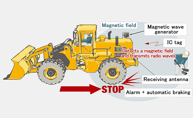
We are adopting the latest technologies to address accident risks in operating sites. One example is an automatic braking system for heavy machinery. Designed to prevent collisions between heavy machinery and people, it combines a magnetic field emitting device on the heavy machinery with RFID tags worn by workers. It can detect people quickly and stop the heavy machinery, without being affected by obstacles in the way.


