News Release
FY2026
June 16, 2026
JX Advanced Metals Corporation
Decision on Capital Investment Policy to Significantly Expand InP Substrate Production Capacity
- Up to JPY 120 Billion Investment Planned Over Four Years to Meet Growing Data Center Optical Communications Demand -
JX Advanced Metals Corporation (President: Hayashi Yoichi, hereinafter "the Company") has decided to undertake capital investment of up to JPY 120 billion1) over the next four years in order to further strengthen its production capacity of indium phosphide (InP) substrates, a crystal material used in optical communications. Detailed investment plans will be announced once they have been finalized.
InP, which has the capability to convert electrical signals into optical signals and vice versa, is used in optical transceivers that play a central role in the optical communications field, supporting the large-volume data transmission required by the advancement of AI.
The evolution of AI is progressing at an extremely rapid pace, from "generative AI," which creates new text, images, and program code based on learned data, to "agentic AI," which understands user intent, autonomously collects and analyzes information, as well as plans and executes tasks. Furthermore, initiatives are advancing toward the social implementation of "physical AI," in which AI is embedded in robots and mobility systems to enable autonomous action in the physical world.
Against this backdrop, the volume of data communication required for data both AI training and real-time inference is increasing dramatically, driving further expansion in demand for hyperscale data centers equipped with high-speed, low-latency communication infrastructure. In addition, as AI processing capabilities improve, the application of optical communication technologies is expanding beyond conventional external connections between servers and racks to include high-speed data transmission within servers. As a result, demand for optical communication equipment is growing at a pace significantly exceeding previous expectations.
In response to this expanding demand, the Company has been steadily increasing its production capacity for InP substrates2, 3, 4). Through ongoing dialogue with customers, the Company continues to receive substantial requests for increased supply associated with their capacity expansion plans. As a result, the Company has strengthened its view that demand for these products will expand further beyond previous expectations.
Under these circumstances, the Company has decided to undertake a large-scale investment--the largest ever for this product--to support the stable supply of InP substrates, respond to customer demand, and contribute to the growth of the expanding optical communications infrastructure market, with a view to further expanding its business. Specifically, in addition to the Isohara Works (Kitaibaraki City, Ibaraki Prefecture), where production has been carried out to date, the Company will strengthen its production framework by establishing additional capacity in the Hitachinaka area (Hitachinaka City, Ibaraki Prefecture), with plans to increase production capacity by approximately 7 to 10 times. In parallel, the Company will move forward with discussions with customers regarding price revisions, with the aim of establishing a stable supply framework. We plan to develop this product into a pillar of revenue alongside our flagship semiconductor sputtering target.
The Company plans to fund this capital investment using a portion of the proceeds from the previously issued convertible bonds with stock acquisition rights, net of the amount allocated for the share tender offer5).
Going forward, the Company will continue to promote initiatives aimed at transforming into a technology-based company, as outlined in the JX Advanced Metals Group Long-Term Vision 2040, and will strive to become a global company that contributes to social development and innovation through advanced materials.
Reference
Note 1: The Company's total investment to date, when combined with the capital investments previously announced (see Notes 2 to 4), amounts to approximately JPY 150 billion in scale.
Note 2: July 23, 2025 News Release "Notice Regarding Capital Investment for Increased Production of Crystal Materials (Acquisition of Fixed Assets)"
Note 3: October 8, 2025 News Release "Notice Regarding Additional Capital Investment for Increased Production of Crystal Materials (Acquisition of Fixed Assets)"
Note 4: February 10, 2026 News Release "Notice Regarding Additional Capital Investment for Increased Production of Crystal Materials (Acquisition of Fixed Assets)"
Note 5: May 20, 2026 News Release "Notice Regarding Commencement of Tender Offer for Own Shares"
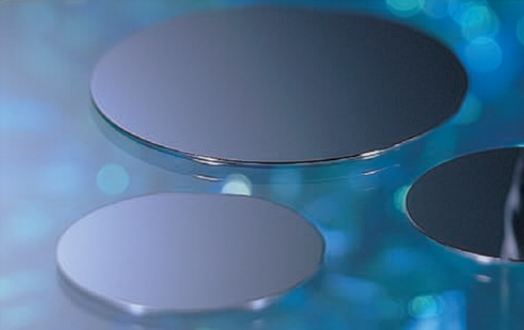
InP Substrate