Fostering the Development and Innovation in Society as a Global Leader of Advanced Materials

Fostering the Development and Innovation in Society as a Global Leader of Advanced Materials
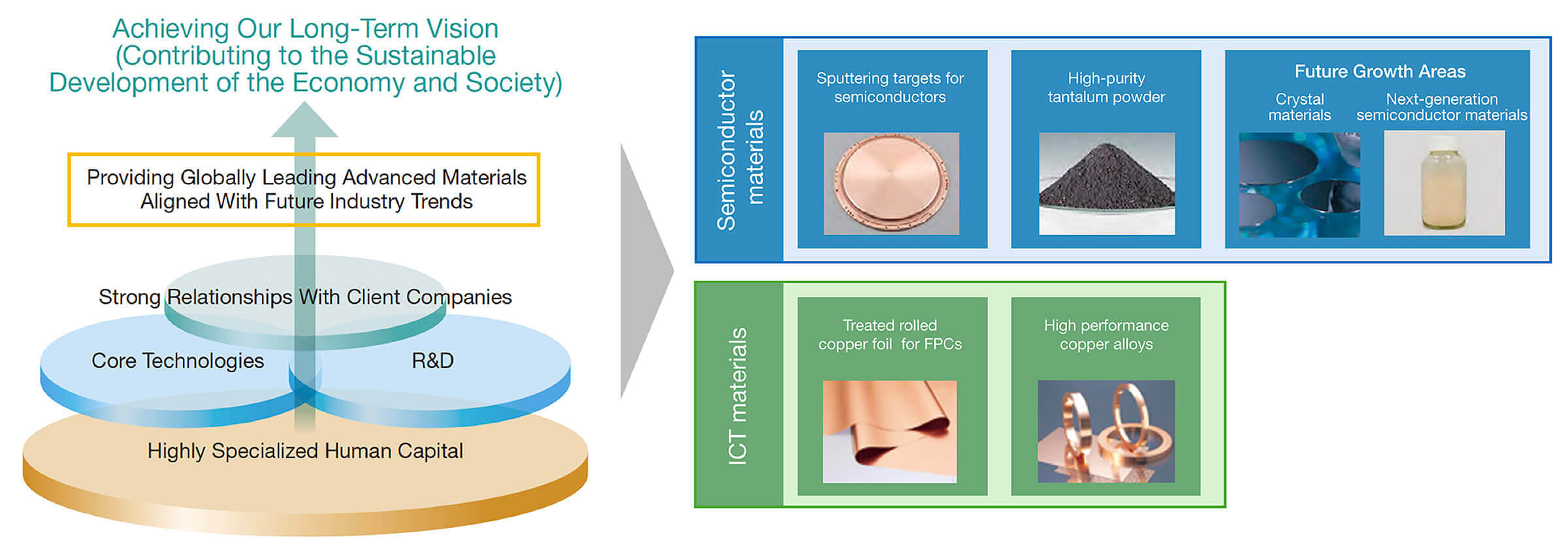
Developing Niche Top Products That Support the Future
The JX Advanced Metals Group develops niche top products that support the future, leveraging a robust R&D structure and elemental technologies cultivated over the 100 years since our founding. We also endeavor to identify new market needs based on strong relationships with customers.
Our Products Supporting Generative AI Demand
AI Server Shipments
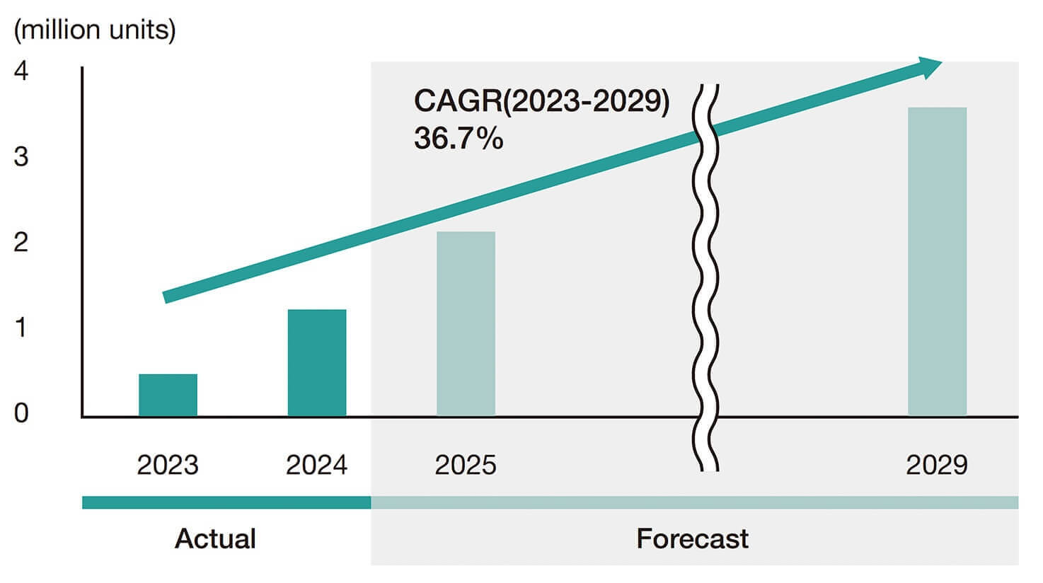
- *Source: Prepared by the Company based on 2025 Prismark Workshop, February 2025, Prismark Partners LLC
Stronger demand is expected for AI servers and GPUs as the spread of generative AI drives advancements in high-speed, high-capacity data transmission. We expect this expansion to lead to significant growth in demand for our sputtering targets for semiconductors, as well as for InP substrates, high-purity tantalum powder, and magnetic material sputtering targets. Demand is also growing rapidly in the ICT materials business for copper titanium alloys used in connectors for AI servers, with current sales volumes rising substantially.
JX Advanced Metals Corporation Product Applications (Data Centers)
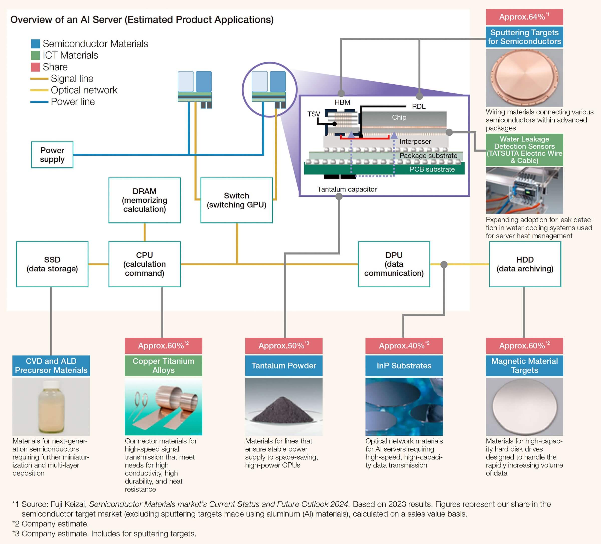
Semiconductor Materials
Sputtering Targets for Semiconductors
Schematic Diagram of Sputtering Target Adoption (Cross-Sectional View of Logic Semiconductor)
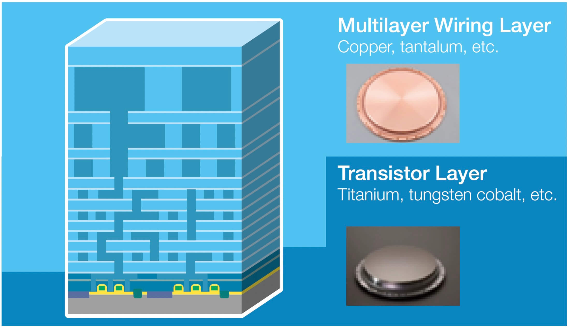
This material is used to form fine wiring within semiconductor devices such as logic and memory devices. We offer a wide variety of sputtering targets, including copper, tantalum, titanium, tungsten, and cobalt, all of which hold the world's No.1* market share.
Semiconductors are becoming increasingly advanced every year, and consequently, there is a demand for high-quality sputtering targets that can form finer wiring. We have established strong relationships built on trust with semiconductor manufacturers and semiconductor equipment manufacturers through the stable supply of high-quality products, and further growth in the scale of our business is anticipated in the future.
- *We prepared this information based on a survey conducted by an external research organization at our request (2021 results based on the sales value of the Company's share of the semiconductor target market).
Point 1
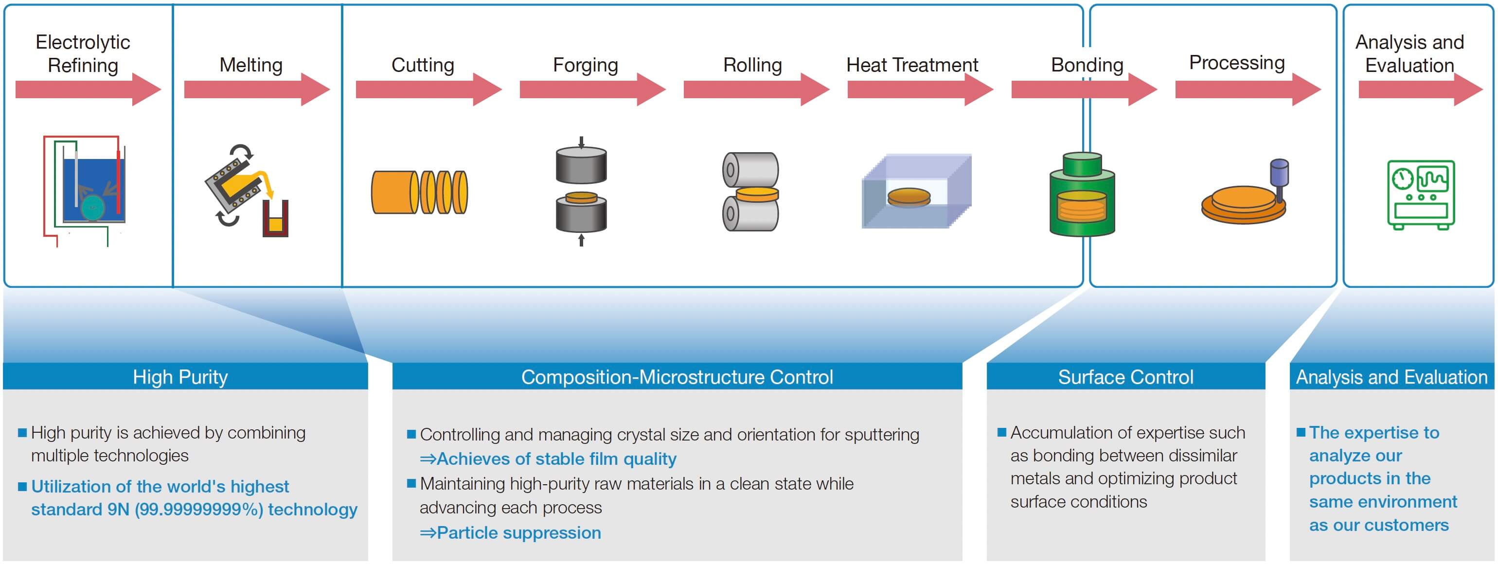
Technological Capabilities that Ensure High Quality and Stable SupplyEven minute impurities can impact defect rates significantly in semiconductor manufacturing, placing extremely high demands on material quality and requires advanced quality control capabilities throughout the entire process. JX Advanced Metals possess advanced technologies and quality control capabilities in across all processes of purification, composition and structure control, surface treatment, and analytical evaluation. These advantages allow us to achieve provide a stable supply of high-quality products across a wide range of metal materials. Our ability to consistently achieve both technological precision and quality across all processes represents one of our key strengths and serves as a barrier to entry for other companies.
Point 2
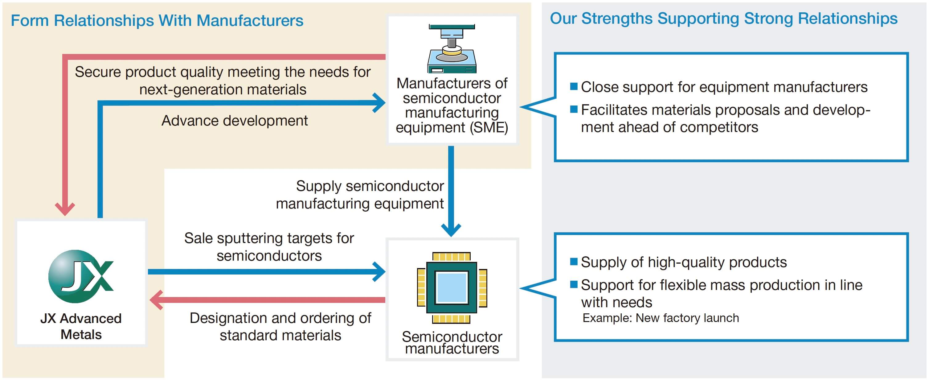
Strong Relationships With Semiconductor Equipment Manufacturers
The JX Advanced Metals business model is supported by strong relationships with semiconductor equipment manufacturers. Designation as a standard material in semiconductor manufacturing equipment is critical to winning orders from semiconductor manufacturers.
We have a long track record of providing a stable supply of high-quality products. Our strong relationships with major equipment manufacturers allow us to propose solutions from the earliest stages of new product development. As a result, our products are often adopted for mass production ahead of competitors, creating a virtuous cycle that represents a significant source of our competitive advantage.
Point 3
Long-Standing Relationships of Trust With Semiconductor Manufacturers (Customers)We have built strong, enduring relationships of trust with our customers through a long track record of providing a stable supply of high-quality products. As a result, we have received numerous awards as an excellent supplier from global semiconductor manufacturers, including Intel and TSMC. These achievements enable us to establish a solid foothold in the semiconductor target market, underpinned by high entry barriers.
Point 4
Global Production SystemWe operate factories in regions where major semiconductor manufacturers operate manufacturing facilities, including Mesa, Arizona, Taiwan, and South Korea. This global mass-production framework enables us to respond flexibly to rapidly changing demand from semiconductor manufacturers.
Manufacturing Process for Semiconductor Sputtering Targets
Business Model Diagram for Semiconductor Sputtering Target Products
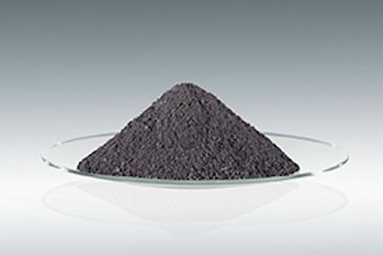
Tantalum and Niobium Materials
The Group acquired shares of H.C. Starck Tantalum and Niobium GmbH (now TANIOBIS GmbH, headquartered in Germany) in July 2018. TANIOBIS supplies world-class tantalum and niobium powders for capacitors, semiconductor materials, and SAW devices, supported by strong technological capabilities and robust marketing strength. As the full-scale IoT era approaches and the number of electronic components and devices in use is expected to rise sharply, against this backdrop, we will support growth in the IoT sector by combining the technologies and expertise of JX Advanced Metals and TANIOBIS to ensure a stable supply of high-quality materials that meet customer needs.
Products
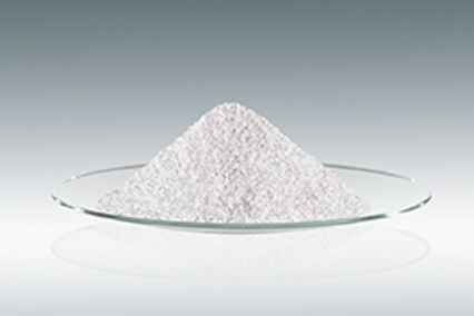
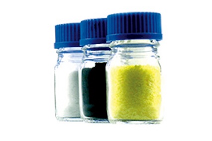
Alloying agents
(1) Crystal Materials
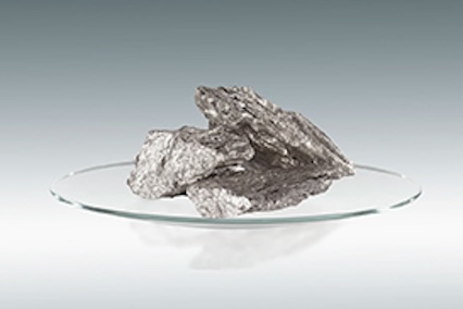
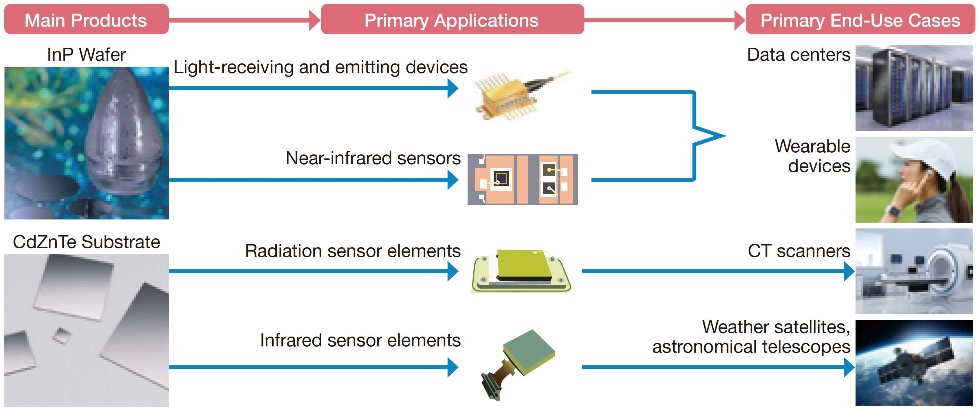
The crystal materials business mainly produces compound semiconductors, including indium phosphide (InP) and cadmium zinc telluride (CdZnTe). We aim to expand this business to accelerate growth in the Semiconductor Materials segment by leveraging the long-cultivated technologies of the JX Advanced Metals Group.
InP is used as a material for light-receiving and emitting devices in optical communications and for infrared sensors, both of which are expected to see strong growth driven by the increasing data traffic from data centers and mobile communications.
CdZnTe is used as a material for radiation sensors and infrared sensor elements, and is expected to grow in fields such as defense and healthcare.
Crystal Materials Business
(2) Next-Generation Semiconductor Materials
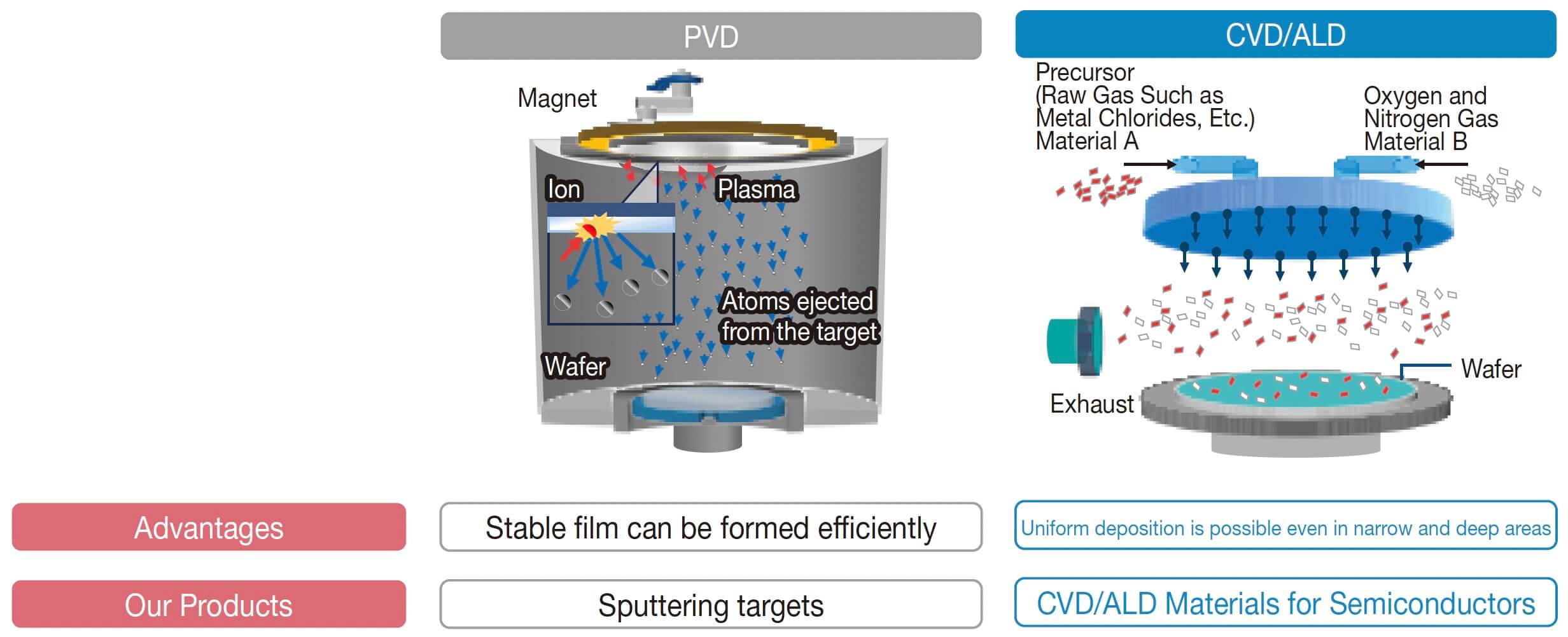
Our next-generation semiconductor materials business manufactures materials used in chemical vapor deposition (CVD) and atomic layer deposition (ALD) processes.
Markets for data centers and AI-enabled IoT devices expand as generative AI continues to evolve, and high-performance semiconductors required for these applications demand further reductions in size and multilayering to achieve higher levels of integration.
The push for finer features and more multilayer structures is increasing demand for thin-film formation using CVD and ALD. In response, JX Advanced Metals is establishing mass-production lines for CVD and ALD materials and strengthening facilities for new process and material development to further expand production capacity.
Comparison of PVD and CVD/ALD Methods
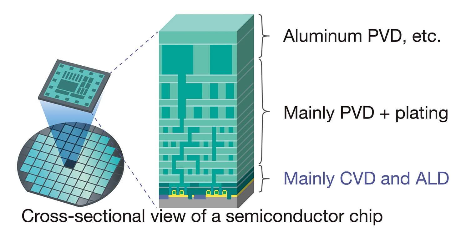
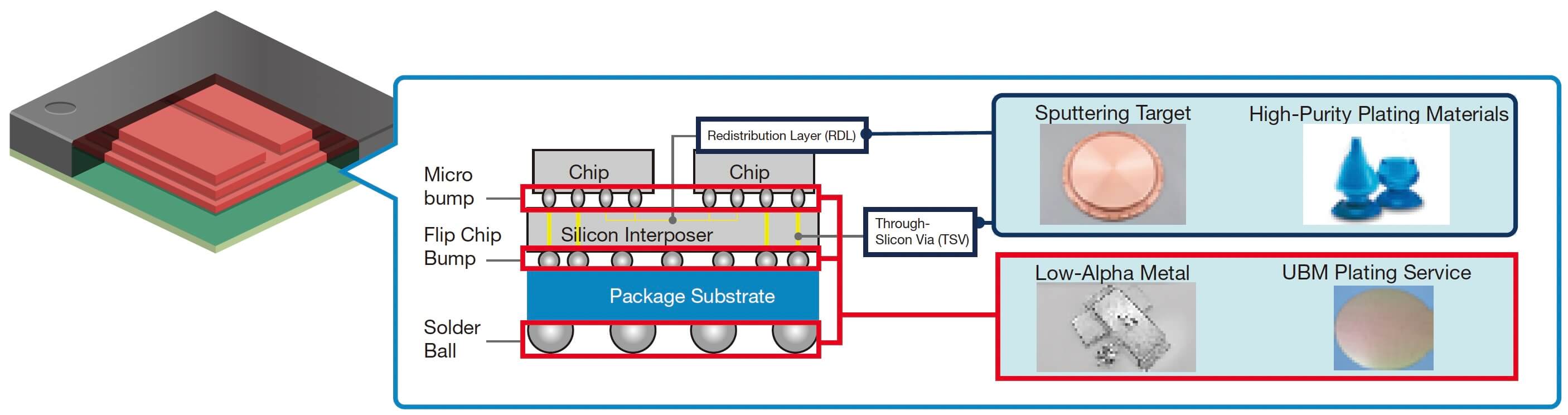
Packaging and Assembly
Discussions about the limitations of enhancing semiconductor performance as an extension of conventional technologies continue. As a result, there is growing attention on post-processing innovations such as chiplets, which significantly increase processing speed through high-density integration of multiple chips with different functions—such as CPUs and memory— on a single substrate. Demand for our sputtering targets is expected to grow as a material for wiring that connects chiplets both vertically and horizontally. The need for new materials, such as high-purity plating materials, is also expected to expand for these applications. Furthermore, an increase in demand for our materials is also anticipated in applications such as materials for mounting semiconductors onto circuit boards.
Cross-Sectional Diagram and Examples of Our Expected Materials and Services
ICT materials
Example of the Adoption of Rolled Annealed Copper Foil
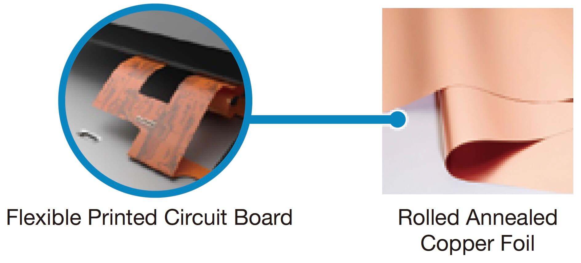
Treated rolled copper foil for FPCs
Treated rolled copper foil is used in flexible printed circuit boards (FPCs). This copper foil is a wiring material that can be bent to connect components inside smartphones, contributing to miniaturization and longer life. In the future, in addition to the further advancement and miniaturization of components for smartphones and PCs with the incorporation of AI, the use of these components is expected to expand through wearable devices such as smartwatches and smart glasses. We have secured our position as a leading vendor, maintaining a competitive advantage through a market development approach that allows us to launch products ahead of competitors by identifying development needs quickly based on strong relationships with end users.
- *Source: 2023 Handbook of New Materials for Electronics Implementation, Fuji Chimera Research Institute (2022 results; for FPCs only; based on shipping volume)
Point 1
The Superior Bending Resistance of Our Treated Rolled Copper Foil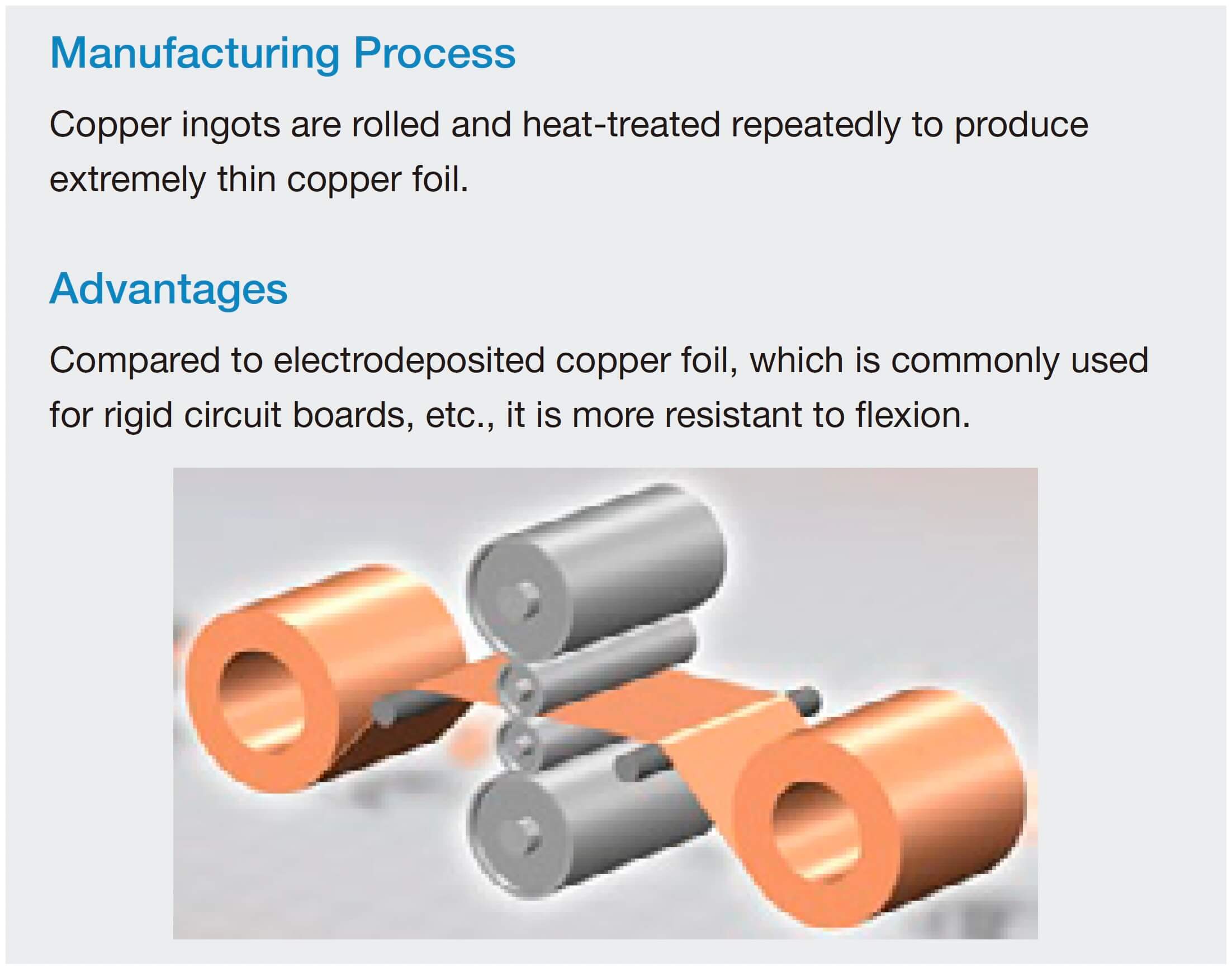
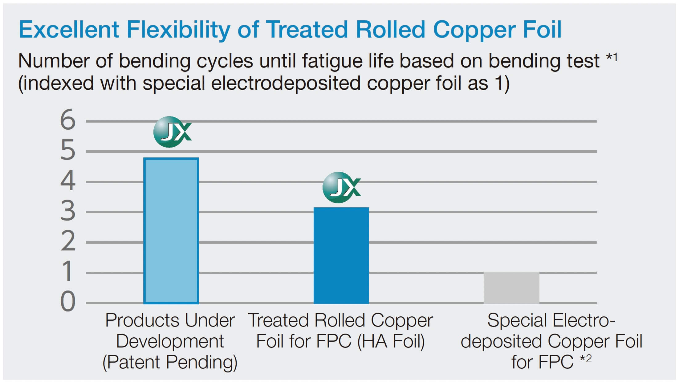
- *1Standard test method for FPC bending resistance in accordance with the standards set by IPC Association Connecting Electronics Industries (a printed circuit industry organization in the U.S.) and JIS standards.
- *2Electrodeposited copper foil that corresponds to Grade 10 Electro-deposited low temperature annealable of the IPC standard IPC-4562A, Metal Foil for Printed Board Applications, which is the most widely used standard in the printed circuit industry globally.
Point 2
Market Development Approach for Early Identification of Development Needs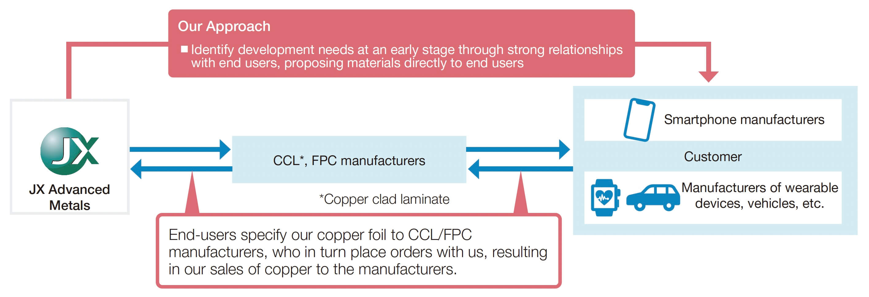
FPCs, one of the main applications of rolled copper foil, are circuit boards that form electrical circuits on base materials (FCCL) made by bonding treated rolled copper foil, a conductive metal, with thin, flexible, and insulating base films such as polyimide. Treated rolled copper foil is used in narrow gaps and moving parts that bend repeatedly, requiring excellent flexibility and durability. JX Advanced Metals leverages proprietary technology and advanced manufacturing expertise to produce high quality, ultra-thin rolled copper foil as thin as 6 micrometers (about one-tenth the thickness of a human hair) for FPC applications.
We have built strong relationships with end-users of treated rolled copper foil for FPCs for over 20 years. Engaging in dialogue with these end-users has allowed us to identify their development needs at an early stage and propose materials based on those needs. Our products receive material specifications directly from end users, which enable stable orders from the CCL and FPC manufacturers supplying those end users.
Property Map
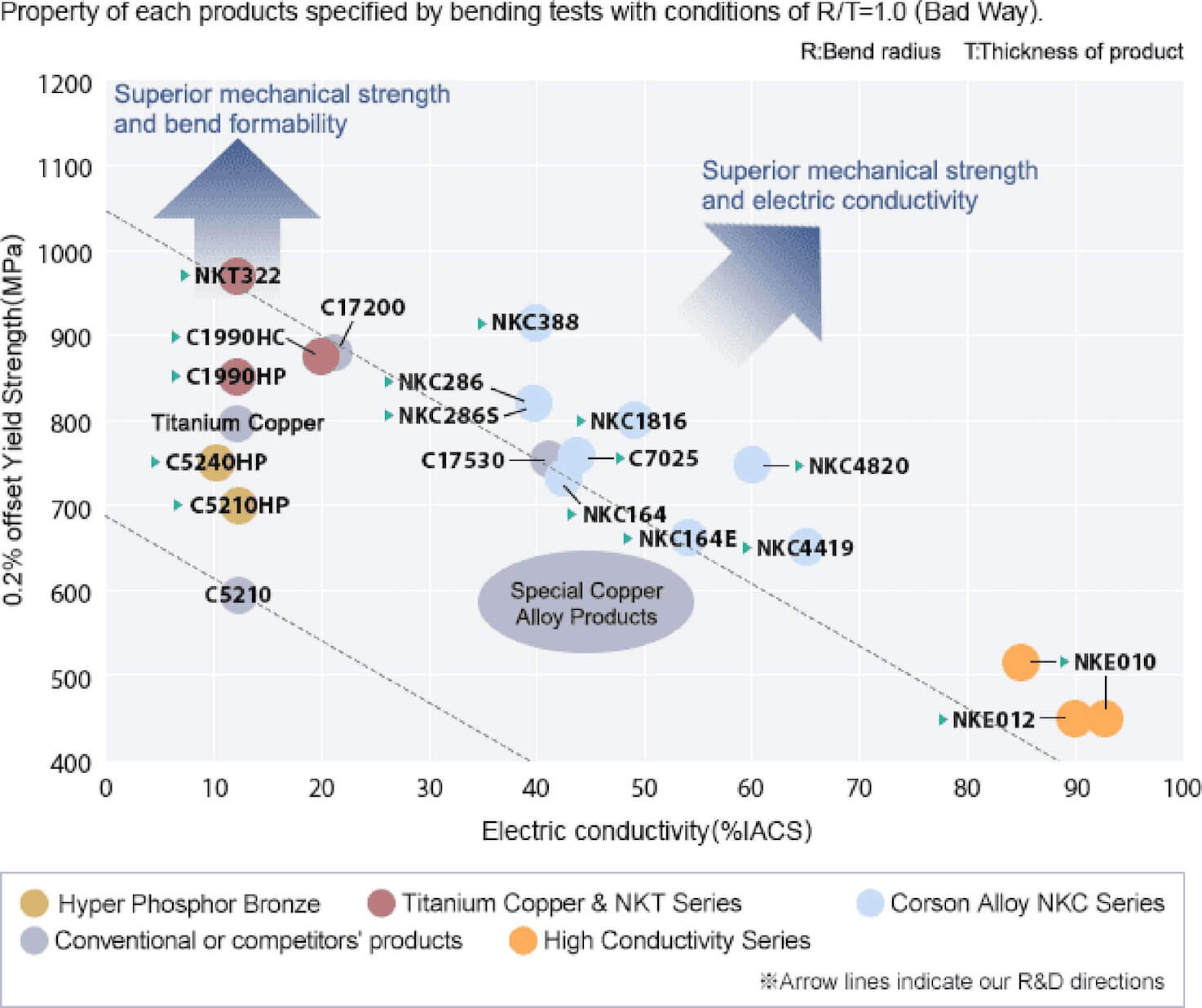
High-Performance Copper Alloys
Our high-performance copper alloy strips, manufactured with precision process control technology, are highly valued in the electronics market for their strength, bendability, and electrical conductivity, we offer a wide range of products that meet demanding customer requirements not only in the IT field but also for automotive electrical components, where electronics adoption continues to advance rapidly.
Reinforcement of Production System
In anticipation of future growth in demand for semiconductor and ICT materials, we are actively expanding production capacity for advanced materials in Japan and overseas, with Ibaraki Prefecture being the center of this expansion.
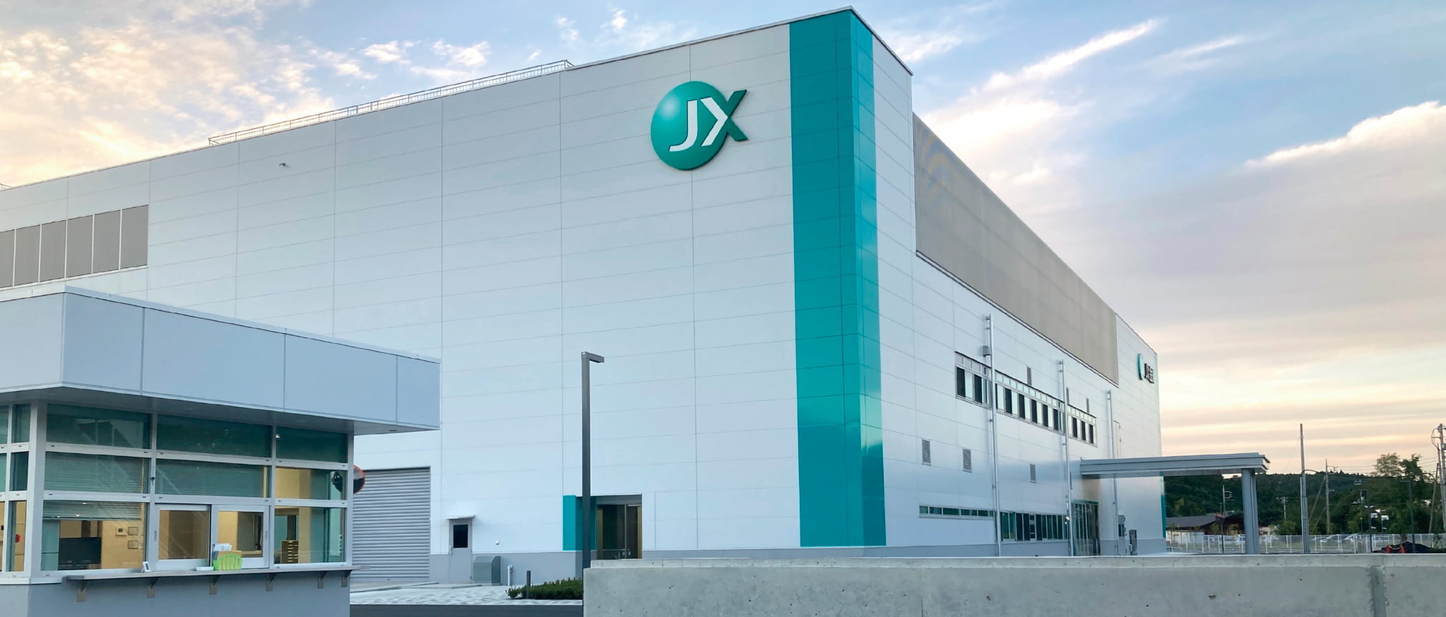
(1) New Hitachinaka Works
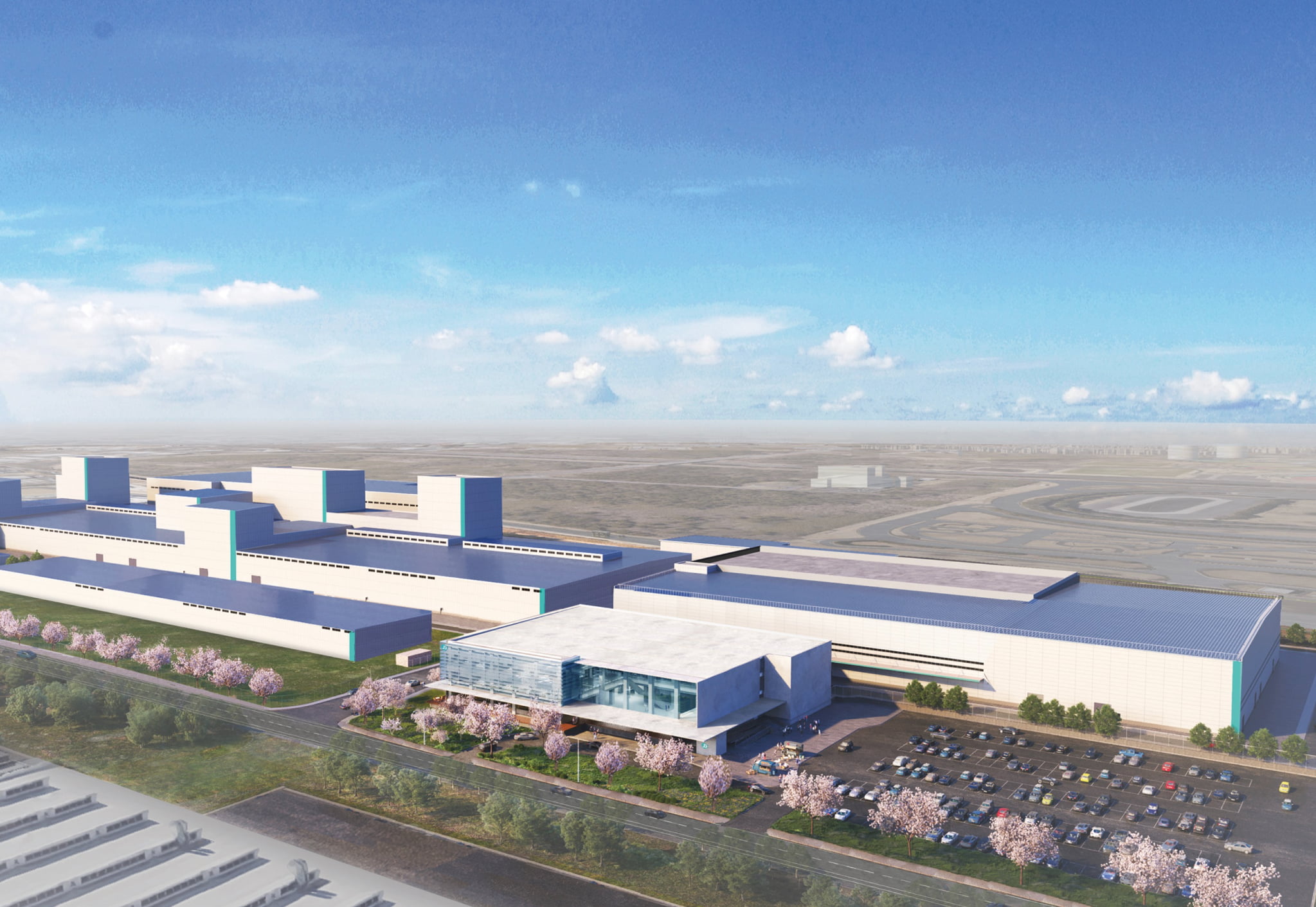
We have acquired a large site in Hitachinaka City, Ibaraki Prefecture, and are constructing a new plant.
The new plant will be responsible for the production of semiconductor materials, mainly sputtering targets for semiconductors, in anticipation of a significant increase in future demand. Ultimately, it is projected to become one of our core facilities, employing over 500 people.
| Location |
|
|---|---|
| Area |
|
| Products |
|
| Operation Launch |
|
(2) New Plant in Arizona
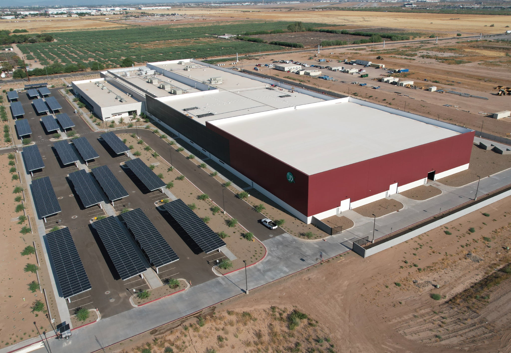
In our new plant located in Arizona, an area of growing concentration in the semiconductor industry, we will flexibly expand production capacity for semiconductor sputtering targets in response to customer requirements. Additionally, we plan to utilize this facility as a base for new business development, establishing it as a hub for advanced business sectors in North America.
| Location |
|
|---|---|
| Area |
|
| Products |
|
| Operation Launch |
|
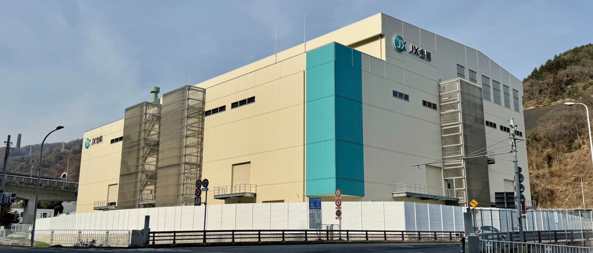
(3) Two New Plants in Hitachi City, Ibaraki Prefecture
To enhance production capacity for semiconductor sputtering targets and treated rolled copper foil, we constructed two new plants in Hitachi City, Ibaraki Prefecture.
| Location |
|
|---|---|
| Area |
|
| Products |
|
| Operation Launch |
|
| Location |
|
|---|---|
| Area |
|
| Products |
|
| Operation Launch |
|
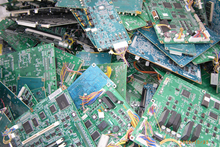
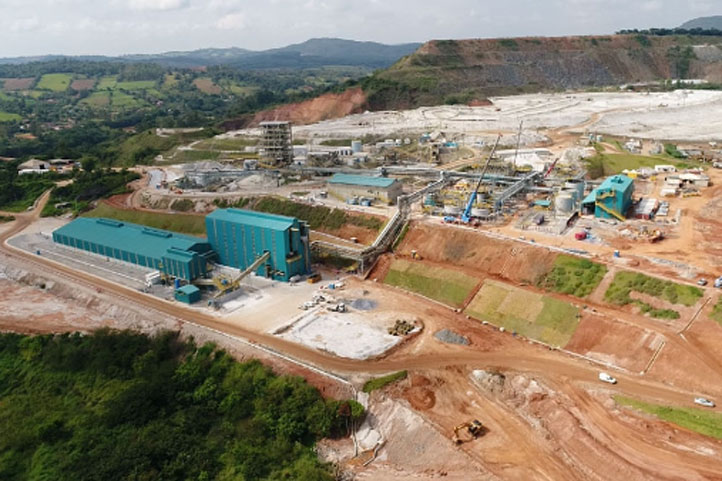
Basic materials (Base Businesses supporting advanced materials)
Rising geopolitical risks are heightening the need to secure stable supplies of precious and minor metals, which serve as essential raw materials in our semiconductor materials.
The Metals & Recycling segment works to further enhance recovery from conventional recycled raw materials, in addition to developing minor metal mines.