News Release
FY2025
September 3, 2025
JX Advanced Metals Corporation
Participating in "JOINT3" Consortium to Develop Next-Generation Semiconductor Packaging
―Accelerating the Creation of New Businesses in the Advanced Packaging Domain―
JX Advanced Metals Corporation (President: Yoichi Hayashi, hereinafter "the Company") has joined "JOINT3" consortium to develop next-generation semiconductor packaging.
JOINT3 is a co-creation evaluation framework established by Resonac Corporation (President and CEO: Hidehito Takahashi, hereinafter "Resonac") with the aim of accelerating the development of materials, equipment, and design tools optimized for panel-level organic interposers through collaboration among material, equipment, and design companies. JOINT3 brings together global leaders in semiconductor supply chain. Using a prototype line for 515 x 510mm panel-level organic interposers, the consortium promotes the development of materials, equipment, and design tools optimized for panel-level organic interposers.
Our company offers a wide range of advanced materials that hold a significant share in the global market, including sputtering targets for semiconductor used in cutting-edge semiconductor manufacturing, indium phosphide compound semiconductor substrates experiencing rapidly increasing demand as materials for AI data centers, titanium-copper alloy foil, and high-purity tantalum powder. Among these, sputtering targets for semiconductor are expected to see expanding demand not only in front-end processes but also in chip-to-chip interconnect formation, which is part of the packaging process. In addition, we provide various products such as surface treatment agents that are anticipated to find applications in this field. Moving forward, we will collaborate with fellow members of the JOINT3 consortium to drive the creation of new businesses in the advanced packaging domain.
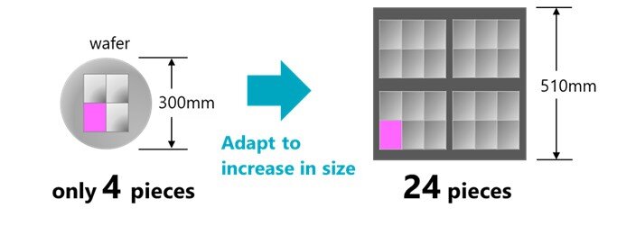
In recent years, packaging for back-end processes has emerged as a key technology in the field of next-generation semiconductors. This includes 2.xD packages, whereby multiple semiconductor chips are arranged in parallel and connected via interposers, demand for which is expected to grow in line with the need for increased data communication capacity and speed. As semiconductor performance improves, interposers are becoming larger, and there is a shift from silicon interposers to organic interposers made from organic materials.
Conventional manufacturing methods involve cutting rectangular pieces from circular wafers. However, as interposers increase in size, the number of them that can be obtained from a single wafer decreases, posing a significant challenge. To address this issue, a manufacturing process that transitions from circular wafer shapes to square panel shapes is gaining attention, as it allows for an increased number of interposers to be produced from a given area of wafer.
In the advanced packaging domain, where no clear de facto standards have yet been established, gathering and analyzing market intelligence is critically important for identifying future technological directions. JOINT3 presents opportunities for collaboration with equipment manufacturers and materials suppliers from diverse sectors. We see it as a valuable platform for gaining cross-industry insights and as a co-creation space where diverse product development take place. This enables us to deepen insights that inform our technological development and product strategy, allowing us to pursue innovation that more closely aligns with market needs. In November 2024, we established a new organization that integrates the marketing and development functions for advanced packaging materials across the group1). This centralized structure enables us to respond to market demands with greater speed and agility.
In advanced packaging technology, where miniaturization and high-density integration continue to progress, the speed at which market-driven proposals can be delivered is becoming increasingly critical--alongside material reliability. Through our participation in JOINT3, we will leverage collaboration with fellow member companies to further accelerate the development and practical application of new materials, drawing on our core technologies and rapid proposal capabilities.
We will continue to contribute to social progress and innovation as a global leader in advanced materials.
![]()
JOINT3 Logo
Reference
1) News release dated October 31, 2024: "Announcement of Organizational Changes"
Overview of JOINT3
| Name | JOINT3 (JOINT:Jisso Open Innovation Network of Tops) |
| Objectives | Accelerate the development of materials, equipment, and design tools optimized for panel-level organic interposers through co-creation with participating companies. |
|
Participating Companies (listed in alphabetical order) |
27 companies (as of September 3, 2025) |
| Location | - Advanced Panel Level Interposer Center "APLIC" (Yuki City, Ibaraki Prefecture, Japan (within the Resonac Shimodate Plant (Minami-yuki))) - Packaging Solution Center (Kawasaki City, Kanagawa Prefecture, Japan) |
| Activities | - Developing materials, equipment, and design tools for organic interposers using a panel-level (515 x 510 mm) prototype production line - Promoting development through co-creation by having material and equipment manufacturers produce common prototypes - Utilizing JOINT3 as a "training ground" for technology and equipment manufacturers to further enhance technologies related to panel-level organic interposers |
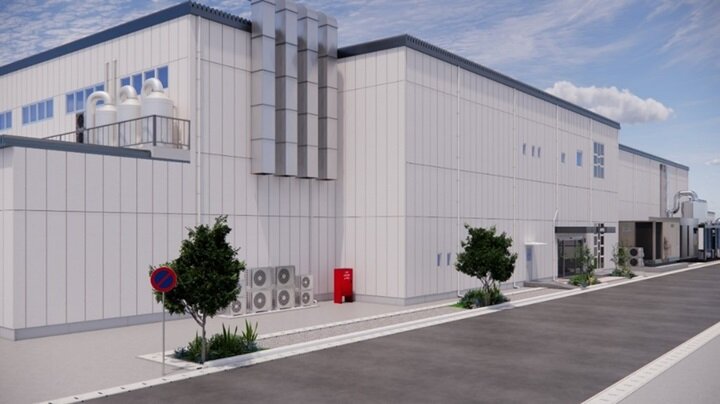
The APLIC building (exterior image)