Pursuing Open Innovation

Pursuing Open Innovation
We are promoting co-creation in a variety of formats, including collaboration with unique technologies held by Group companies, joint research with universities and other research institutions, and partnerships with external companies. These activities aim to build a system for generating new technologies and value.
Collaboration for the Social Implementation of Innovative Semiconductor Fabrication Technology
We have invested in Gaianixx, a start-up company from the University of Tokyo, and have started collaborating with them to explore new developments in the crystal materials business.
Semiconductor devices such as power semiconductors that have revolutionized the power supply systems of electric vehicles use crystal materials consisting of functional thin films layered on a single-crystal substrate. However, to achieve even higher performance and added value, addressing the strain that occurs between the single-crystal substrate and the functional thin film has become a key challenge. Gaianixx aims to address this challenge with its proprietary Multi-Functional® interlayer technology. The practical application of this technology is expected to lead to a revolutionary improvement in the performance, reliability, and yield of semiconductor devices. With this investment, we plan to jointly develop materials such as sputtering targets used for functional thin films and high-purity metals, as well as stacked crystal materials.
Accelerating the Social Implementation of Printed Electronics

Through collaborative research with the National Institute of Advanced Industrial Science and Technology (AIST), we are advancing development of fine wiring technology for next-generation devices using printed electronics (PE). PE is a technology that forms wiring by printing ink containing conductive materials onto resin films or glass substrates. It is said to enable finer wiring than the wiring formation using copper foil etching methods, and it is expected to contribute to the further miniaturization and thinness of devices such as smartphones and wearables.
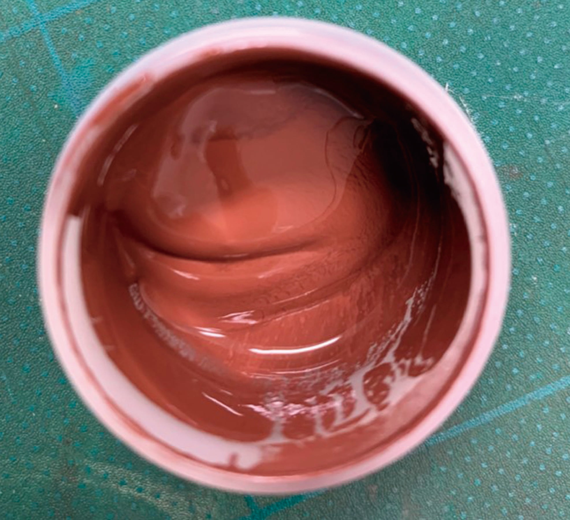
By combining our copper ink technology using copper micropowder with AIST's printing technology, we have made it possible to form fine copper wiring. Having achieved the formation of fine copper wiring with a line width of 6 µm, the finest level in the world using screen offset printing technology*, we have officially launched marketing activities aimed at social implementation. Moving forward, we will gather feedback through dialogue with our customers and continue to explore various applications.
- *Screen Offset Printing Method: A technique where conductive ink is screen-printed onto a transfer medium, and then the printed conductive ink is transferred to a substrate for formation. The process is simple, large-area printing is easy, and the printing speed is fast.
Advancing Development of Semiconductor Material Mg2Si Single Crystal for Optical Sensing Technology

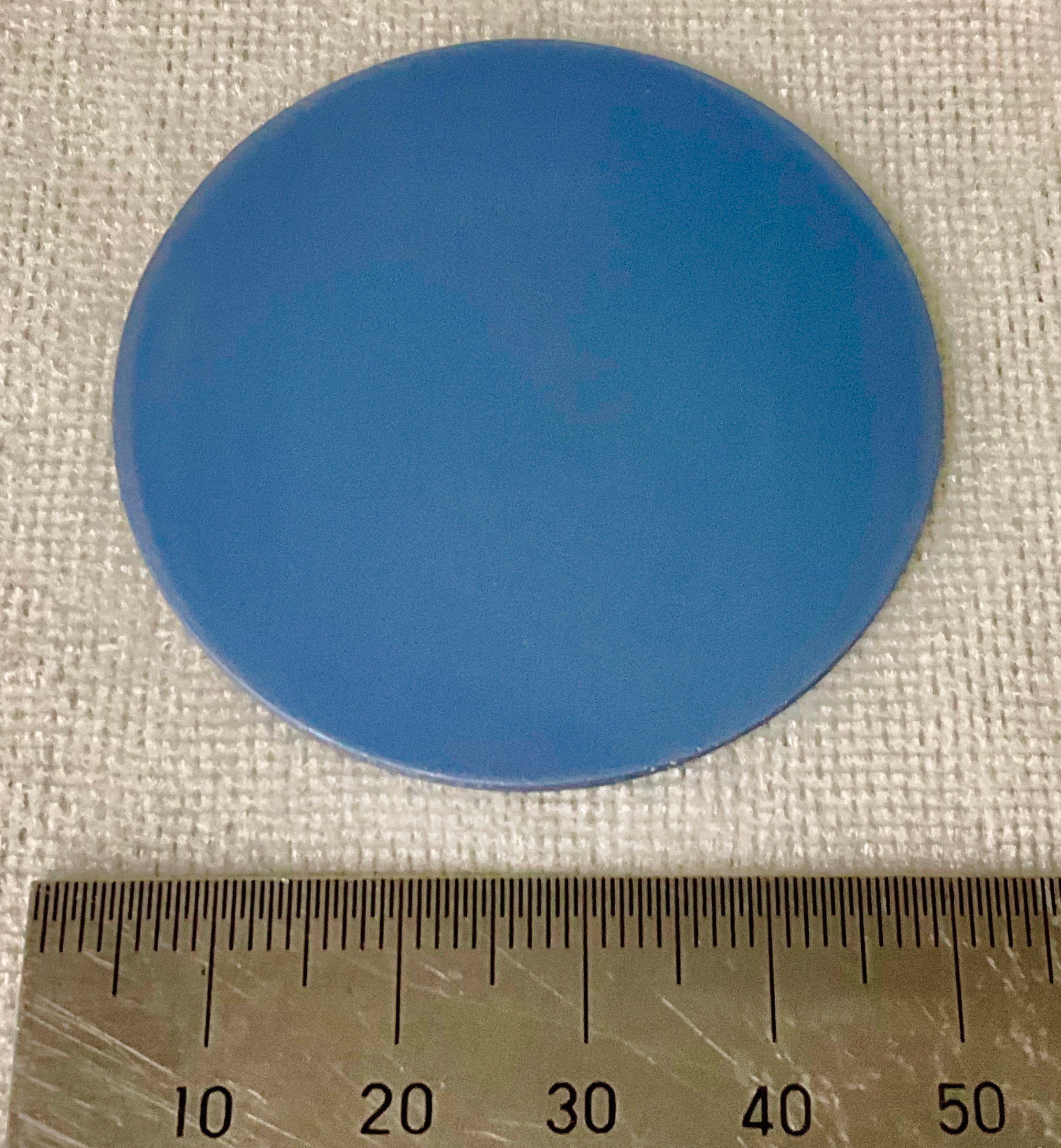
We are conducting joint research with Ibaraki University's College of Engineering on magnesium silicide (Mg2Si) single crystal, a semiconductor material that will be used in next-generation optical sensing technology. Optical sensing technology is expected to be used in a wide range of fields such as industrial inspection, healthcare, disaster prevention and security, and autonomous driving in automobiles.
The Mg2Si single crystal, which Professor Udono Haruhiko of the College of Engineering at Ibaraki University and the Company are working on developing, can detect light in a wide range of wavelengths from visible light to shortwave infrared. Additionally, because it utilizes a widely available material, the Mg2Si single crystal achieves a balance between performance and cost-effectiveness. In the collaborative research, we are working to increase the size and quality of Mg2Si single crystals.
We are promoting marketing activities aimed at the social implementation of this product, raising awareness of the product through exhibits at trade shows, etc., and fostering communication with manufacturers involved in the production and development of semiconductor devices.
Activities of the JX Advanced Metals Endowed Unit

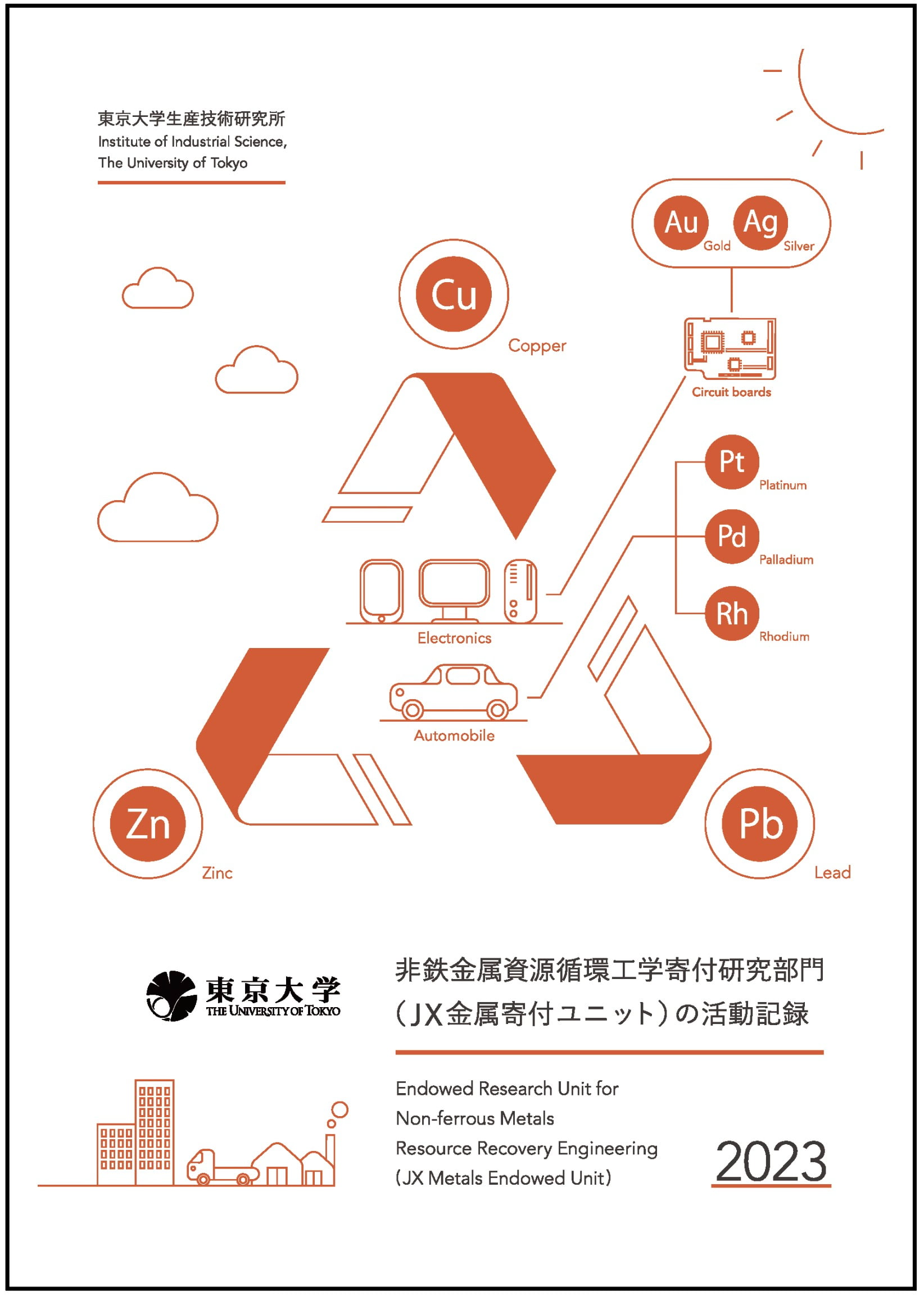
Despite growing needs for a stable supply of nonferrous metal materials in recent years, the pool of researchers and engineers in Japan working in fields related to smelting, refining, and recycling nonferrous metals has been on the decline. In response to this situation, JX Advanced Metals, in collaboration with the Institute of Industrial Science, the University of Tokyo, launched the Endowed Research Unit for Nonferrous Metal Resource Recovery Engineering (JX Advanced Metals Endowed Unit) in 2012. The purpose of this organization is to develop new environmentally friendly recycling technologies for nonferrous metals while also developing the human resources responsible for the work in this field.
The unit began Phase 3 (five years) in January 2022. In Phase 3, we are developing activities to promote a further understanding and awareness of the importance and future of the nonferrous metals industry, as well as focus on activities for realizing the SDGs and for STEAM education* to nurture the next generation.
- *STEAM education: An educational concept that combines the initial letters of five words: Science, Technology, Engineering, Art, and Mathematics. This concept aims to develop logical thinking and creative skills that lead to problem-solving in the real world

Symposium on Industry–Academia Collaboration and Human Resources Development
On September 20, 2024, the Endowed Research Unit for Nonferrous Metal Resource Recovery Engineering (JX Advanced Metals Endowed Unit) held the Symposium on Industry–Academia Collaboration and Human Resources Development at the Convention Hall of the Institute of Industrial Science at the University of Tokyo.
On the day of the event, Project Professors Yamanaka Shunji, Kurokawa Harumasa, Sugano Tomoko, and Tokoro Chiharu, along with Project Lecturer Ouchi Takanari from the Endowed Unit, gave lectures on industry–academia collaboration and efforts to develop and secure talent through cooperation between companies and universities. Yamaoka, Manager for Open Innovation in the Company Advanced Technology & Strategy Department, Technology Group, introduced JX Advanced Metal activities for students and the platform that supports employee ideas. The event drew many participants and created a lively atmosphere.
12th Symposium on Precious Metals
The JX Advanced Metals Endowed Unit held the special joint 12th Precious Metals Symposium Frontier of Extraction and Recycling Technology for Precious Metals on January 10, 2025. This symposium aims to expand personal exchanges through discussions in the field of precious metals extraction and recycling. Senior Engineer Yamaguchi Yosuke of the Company Technology Department, Metals & Recycling Division, gave a lecture titled Se and Te Recovery in the JX Advanced Metals Precious Metal Recovery Process. Approximately 200 participants from industry, government, and academia, primarily from precious metals-related companies, attended the event, resulting in lively discussions.
JX Advanced Metals Endowed Unit
Members (FY2024)*Positions as of April 2024, reproduced from the website
Project Professor
Okabe Toru H.
- Vice President, The University of Tokyo
- Professor, Research Center for Sustainable Material Energy Integration, Institute of Industrial Science, The University of Tokyo
Project Professor
Tokoro Chiharu
- Professor, Faculty of Science and Engineering, Waseda University
- Professor, Graduate School of Engineering, The University of Tokyo
Project Professor
Kurokawa Harumasa
- Advisor, Sumitomo Metal Mining Co., Ltd.
- Outside Audit & Supervisory Board Member, Sumitomo Mitsui Construction Co., Ltd.
Project Professor
Yamanaka Shunji
- University Professor, The University of Tokyo
- Project Professor, Design-Led X Promotion Platform, Institute of Industrial Science, The University of Tokyo
Project Lecturer
Narumi Taka
- Lecturer, Institute of Industrial Science, The University of Tokyo
Main Activities in FY2024
- September 20, 2024 Symposium on Industry–Academia Collaboration and Human Resources Development (organized by JX Advanced Metals Endowed Unit)
- January 10, 2025 12th Precious Metals Symposium Frontier of Extraction and Recycling Technology for Precious Metals (organized by JX Advanced Metals Endowed Unit)
