Corporate Overview
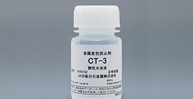
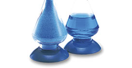
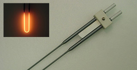
Products and Services
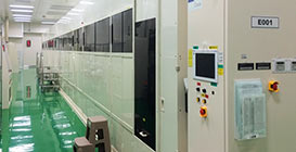
Research and Development
Investors
Management Information
Performance/Financial Information
IR Library
Stock Information
Other IR Information
Sustainability
News
MENU