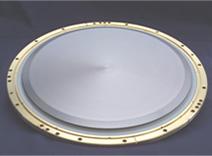
Sputtering Target (PVD) for Semiconductor
To meet the growing demands of today's devices for lower power use and faster processing, the semiconductors making such performance gains possible require various kinds of high-quality targets.
We deliver sputtering targets for semiconductors - products for which high purity is a key requirement - by means of highly stable processes extending from mass production products to specially developed products.
What's more, our well-equipped manufacturing and service sites in Japan and throughout the world enable timely technical, sales, and delivery support.
Features
- These targets embody a wealth of metal product manufacturing technology, including high purity and alloying technology.
- Even large targets achieve uniform properties.
- Comprehensive quality assurance and technical services are provided, making use of many kinds of analysis and evaluation equipment.
- Our four worldwide processing plants help us offer flexible delivery dates and maintain business continuity.
- Our development teams are well able to carry out a balanced range of tasks from research to technical service and prototyping.
Technology and Properties
- Manufacturing sites
- Upstream processes and machining: Isohara Works (Ibaraki Prefecture)
Machining: USA, South Korea, Taiwan
- Marketing and business offices
- Tokyo, USA, Taiwan, South Korea, Singapore, Germany, China
- Products handled
- Various sputtering targets for semiconductors
Sputtering chamber coils, etc.
- Evaluation and analysis equipment (examples)
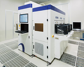
- Sputtering equipment for 300 mm wafer
- Quality system (certified)
- ISO9001
ISO/TS16949
ISO14001
Main Products Handled
Various targets are available, offering the high purity that makes devices more reliable.
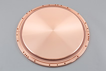
Ti Target
Our Ti targets are widely used in places where titanium is necessary in semiconductors, such as barrier layers for Al interconnects, and hard masks. With the presence of Toho Titanium Co., Ltd., manufacturer of high-purity titanium, the Group has a full supply chain from raw material to target.
Features
- We have built up a wide-ranging lineup of different shapes through 20 years of experience.
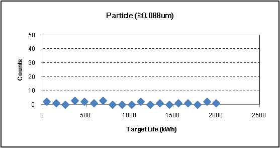
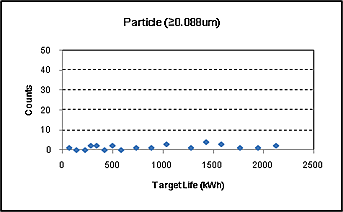
- Measures are taken to minimize particle levels and shorten burn-in time.
- We have developed materials for high-power sputtering use.
Technology and Properties
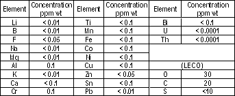
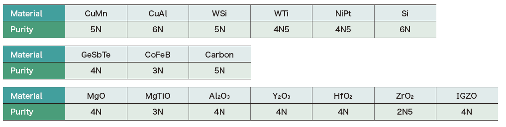
Purity 4N5 (Ti 99.995% or above)
5N
5N5
Shapes ---Support for all sputtering equipment and wafer sizes.
SFG and SR made standard specifications ---To minimize particle levels and shorten burn-in time
Uses
- Interconnect barrier
- Hard masks
- Gate electrodes
- UBM
- TSV, etc.
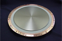
Cu target

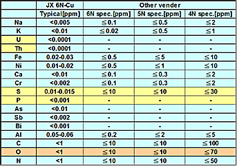
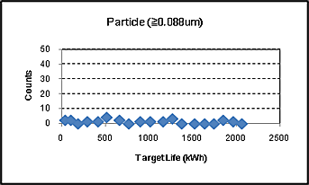
Our Cu target, with 6N (99.9999% or above) purity, was specially developed to reduce particulate matter during sputtering. JX Advanced Metals encompasses the entire supply chain, from resource extraction, smelting and refining to target manufacturing, enabling reliable supply of our world-standard 6N target.
Features
- High-purity targets are supplied as standard products thanks to in-house smelting and refining.
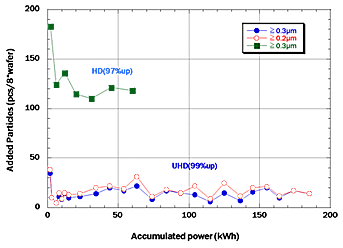
- Particle reduction is remarkably effective.
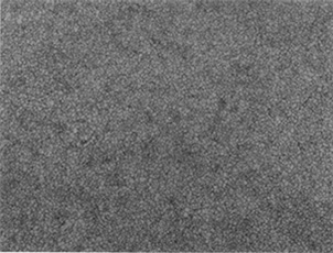
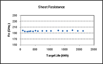
- Uniform grain diameter helps stabilize sputtering data.
Technology and Properties
Purity 6N (99.9999% or above). Note that 4N5 product is available for applications other than semiconductor interconnects. All sputtering equipment can be used for any wafer size. Particle suppression is especially effective at reducing O, S, and P impurities.
Applications
- Cu interconnect seed layer
- UBM
- TSV, etc.
Cu alloy target
Exhaustive efforts are made to minimize particle occurrence during sputtering. We use 6N (99.9999%) Cu manufactured at the Isohara Works as the raw material for semiconductor sputtering targets, and a wealth of knowledge about melting with additive metals is incorporated into the processes. Excellent affinity for mass production lets us rapidly launch manufacturing for leading-edge semiconductors using Cu alloy.
Features
- Suppression of particles to a minimum is built into the processes.
- Grain size and alloy composition are uniform on the surface and in the cross-sectional direction.
- We can flexibly respond to requirements for alloy type and composition.
- Support for mass production is outstanding.
Technology and Properties
Alloy types: CuAl, CuMn, etc.
A wide range of requirements for other additive metals and composition can also be met. Feel free to consult with us about requirements for other alloys that do not include Cu.
(Mn concentration: 1at% or below)
Sputtering data
Applications
- Cu interconnect seed layer for leading-edge semiconductors
Ta target
We perform all processes in-house, from upstream processes including forging and rolling down to target manufacturing, using the purest raw materials in the industry. We are thus able to exercise full control over the grain size and orientation that affect sputtering properties. Armed with these advantages, we can flexibly meet detailed customer requirements for quality, as well as delivery dates.
Features
- We provide product design matched to customer quality requirements.
- High purity technology minimizes particle levels.
- Support for mass production is outstanding.
Technology and Properties
Purity 4N5 (effectively 5N or above)
We can meet customer requirements for product thickness, e.g., 0.25", 0.5".
(Use of Trio grade)
Sputtering data
(Use of Trio grade)
Sputtering data
Applications
- Barrier in Cu interconnect process
- For TSV, etc.
Other
- All the Ta raw materials used in our products are third-party certified as not coming from conflict mineral sources.
W target
By using powder sintering to manufacture W targets with purity of 5N (99.999% or above) and density of 99% or greater, we are able to achieve both high quality and mass production. To meet recent demand for high-power sputtering, we also market diffusion bonding products with greater bond strength between the target and backing plate.
Features
- High-purity technology and high density help to minimize particle levels.
- Well suited to mass production.
- Thermal resistance is increased by diffusion bonding.
Technology and Properties
Methods of bonding to the backing plate: In (indium) bonding and diffusion bonding
Applications
- Gate electrodes
Other
- In addition, W-Si and W-Ti targets are available.
Sputtering targets for semiconductor gates
Features
Semiconductor gates demand reliability over the long term, and the same applies to material for manufacturing them. We produce high-purity Co and Ni in our Isohara Works. We continue to supply highly reliable products by using such stable-quality Co and Ni as raw materials and by making use of mass production and alloying technology.
- The high purity helps ensure products are not affected by impurities during long-term use.
- In the case of magnetic materials, the magnetic properties are stable.
- Diffusion bonding is also possible.
- Surface thickness uniformity is excellent.
Technology and Properties
Product (purity) Co (5N = 99.999% or higher)
Ni (5N)
NiPt alloy (4N5), etc.
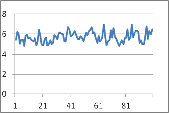
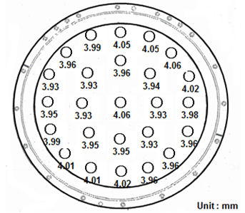
(Co target surface thickness variation)
Applications
- Gate electrodes
Other
- Various other kinds of targets can be provided in addition to the above, for gate electrode and work function adjustment uses.
Contact us about desired types and compositions.
Various coils and parts sets
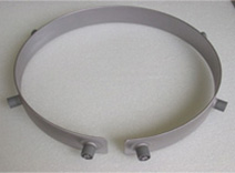
In the Applied Materials equipment used for sputtering for 200 mm and 300 mm wafers, coils and parts sets of the same material as the target are used inside the chamber. We supply these coils and parts sets for Ti, Cu, and Ta.
Features
- We are an officially authorized supplier for the US company Applied Materials, Inc. (AMAT).
Product introduction
Ti 200 mm parts sets (coils, pins, caps)
Cu 200 mm parts sets (coils, pins, inner caps, etc.)
Ti 300 mm coils
Cu 300 mm coils
Ta 300 mm coils
Lineup of Other Targets (examples)
Evaluation Equipment
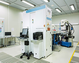
We use the same kinds of sputtering equipment as our customers to confirm quality.
Inquiries accepted 24 hours a day