Products and Services
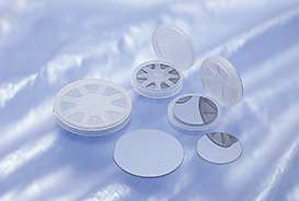
Compound Semiconductors and Crystal Materials
Utilizing the Group's proprietary crystal growing technology, we provide compound semiconductor substrates and crystal materials of various kinds.
InP Substrates
We manufacture InP for III-V compound semiconductors.
CdZnTe (CdTe) Substrates
We manufacture CdZnTe(CdTe) for II-VI compound semiconductors.
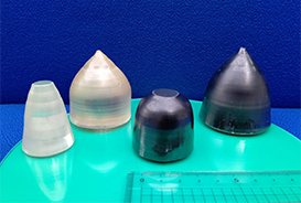
YAG Ceramics for Laser Applications
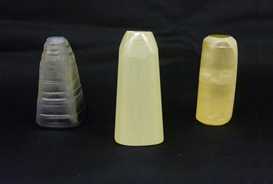
We are developing polycrystalline YAG for laser applications, with the same transmittance as single crystal YAG and larger size.
Strontium Titanate (SrTiO3)

SrTiO3 substrate manufactured by Furuuchi Chemical Corporation.
Rutile Titanium Dioxide (TiO2)

TiO2 manufactured by Furuuchi Chemical Corporation. Available as powder in addition to substrate form.
Contact Information
From the Web
Inquiries accepted 24 hours a day