Sputtering Targets
Sputtering Targets for Transparent Conductive Films

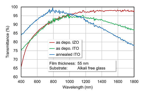
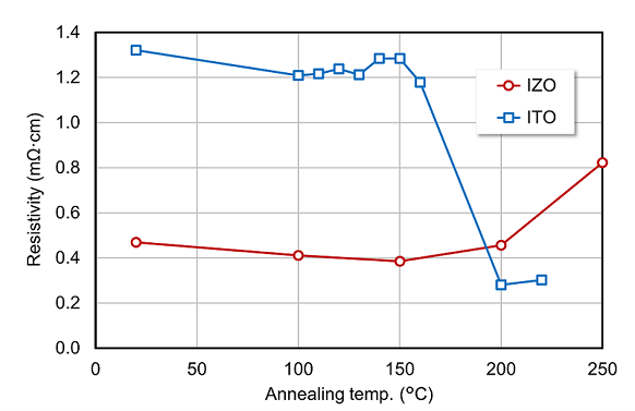
Transparent conductive oxides (TCOs) are widely used as pixel electrodes for LCD and OLED displays or as window electrodes for solar cells due to their transparency and conductivity. Our proprietary TCO, IZO (Indium Zinc Oxide), is expected to be used as a transparent electrode for various infrared devices or CIGS solar cells due to its high transmittance from the visible to the shortwave infrared (SWIR) region. In addition, unlike ITO (Indium Tin Oxide), it does not require annealing after deposition, making it a promising material for OLED or flexible devices.
Product line
IZO sputtering targets, other TCO and various oxide sputtering targets.
Features of IZO
- Superior transparency from the visible to the SWIR region (see Fig. 1).
- Excellent conductivity and transparency without annealing, making possible to deposit on materials with poor resistance against high temperature (see Fig. 2).
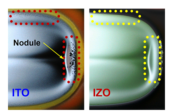
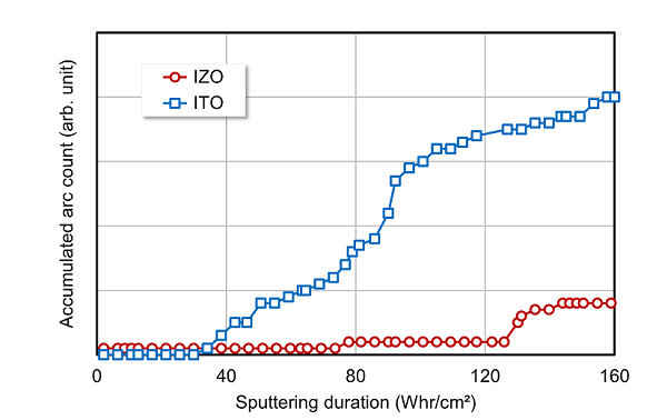
- Low nodule generation during deposition, enabling low-particle processes (see Figs. 3, 4).
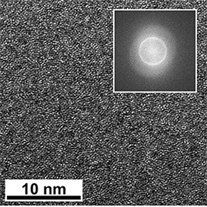
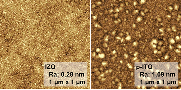
- Amorphous structure lowers the film stress and facilitates the construction of multilayer structures. It also lowers the surface roughness (see Fig. 5).
Applications
- Micro OLED displays,
- SWIR optical devises,
- Wearable devises, etc.
Typical properties of IZO
- Note:The following results were obtained by using in-house equipment and do not guarantee the properties of the product.
Contact Information
From the Web
Inquiries accepted 24 hours a day
