Compound Semiconductors and Crystal Materials
CdZnTe (CdTe) Substrates

JX Advanced Metals products with their consistently high quality are winning customer acclaim and confidence. We manufacture CdZnTe (CdTe) for II-VI compound semiconductors. We supply products meeting the latest demand and product requirements.
| Product name | CdZnTe (CdTe) (Cadmium Zinc Telluride) Substrates |
|---|---|
| Primary Applications | Infrared detectors, radiation detectors |
Lineup
| Size(mm) | Orientation | |
|---|---|---|
| CdZnTe Substrates | 10×10- 95×95 |
(111),(211) |
- CdTe is also available.
| High resistivity CZT Lineup | Size(mm) | Thickness(mm) | Resistivity(Ωcm) | μτ(cm2/V) | Standard pixel design |
|---|---|---|---|---|---|
| Bare substrate | Up to 60x60 | 0.5–5.0 | 107–1011 | Electron: 1x10⁻⁴–2x10⁻³ Hole: 1x10⁻⁵–9x10⁻⁵ |
- |
| Planar detector | Up to 10x10 | - | |||
| Pixel detector | Up to 40x40 | Pixel pitch: 75 μm Pixel size: 50 μm |
Application Examples


Features
- Large-diameter CdZnTe single crystals of the world’s highest quality are achieved using our proprietary crystal growing technology.
- CdZnTe can detect radiation with higher precision than other materials, for stable X-ray detection.
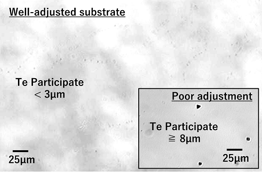
- Our CdZnTe substrates with uniform Zn concentration enable customers to produce larger infrared sensors.


Features of high-resistance CdZnTe substrates for radiation sensor use


(left: planar device; right: pixel electrodes)
- High resistance reduces dark current.
- Polarization does not occur, thanks to the outstanding stability.
- Excellent interoperability with application-specific integrated circuits (ASIC) is possible.
- Can be supplied as bare substrate or with planar device or pixel electrodes.
Contact Information
From the Web
Inquiries accepted 24 hours a day